
INTRODUCTION
The Renewable energy is showing a great ramp up in these early decades of 21st century era. The trends and prediction show a promising future for solar, wind, tidal etc. The solar energy harnessed in the form of solar photovoltaics and heat are boosting ever since the early 2000s, and in the year 2019 it shot to gigantic 25% growth rate and increasing.

Note: A better-edited version of this blog is available in original MS Word format, link below:
https://drive.google.com/open?id=1a63QhjDmNMEEZI1iW9Ik_POmSW0UGre7
Follow for an eminent IEA report “World Energy Outlook 2019” to know all about our planet’s current energy scenario:
https://www.iea.org/reports/world-energy-outlook-2019/renewables#introduction

The problem with renewables is not of power scale but of irregular availability. For example, in a single hour, the amount of power from the sun that strikes the Earth is more than the entire human race consumes in a year, a hurricane every second releases the energy equivalent of 10 atomic bombs but last only a few minutes or hours.

However, it an obvious fact that we couldn’t tap tiny fraction of these mighty energy resources due to present technology constraints, but nothing could be so soothing, to hear of energy availability at such minimal cost to our environment when climate scientist predicts of human race extinction due to fossil-fuel induced climate crisis.
The supply and demand cannot be achieved using renewables without proper engineering. Energy storage provides the only feasible solution to link the two. Storing when excess availability and delivering when demand exceeds generation.
There is massive science community working in the area of energy storage technologies: mega batteries, large pumped hydro storage, thermal storage, chemical storage, etc.
MIT Lecture on future of Energy Storage: https://www.youtube.com/watch?v=E76q-9q7ZDg
Now the other face of story is that the modern power system is in transitional period, now DC power is again gaining ground on consumer side like the highly efficient BLDC motors, semiconductor applications like large database centers, home appliances, and jillion low power devices operating on DC. But still AC is major form of consumption and unfortunately major storage technologies (most importantly batteries) don’t store AC power directly.
And here comes the topic of the blog: The Inverter Circuits.
Inverter Circuits are systems designed for efficient conversion of DC electricity into AC electricity, and comes in wide range of power ratings from small solar charging LED lighting system to medium house emergency system to massive receiving stations of HVDC transmission lines using different conversion principles.
Under this project, team Aantarak aimed to look upon inverter technologies and tried to develop an insightful understanding of the operational principles of inverter circuits, with a vision to further improve the existing technology.
In this first blog intuitive explanation of inverter principle and mathematical analysis of system performance, typically available topologies, major circuit engineering challenges and scope of improvement are explored.
BASIC IDEA OF DC TO AC CONVERSION
Suppose we have V Volts DC battery source and we want to power an AC load whose input is specified as f Hz.
How would you do that, think for a second.
To get an AC supply from a DC source, all we have to do is to interchange the supply terminal across the load at the required rate. So, for 1/2f seconds we are giving +V, then zero and then -V for next 1/2f seconds.

Well that is a square wave.

If you recall the mathematical treatment of waves shapes in previous blogs, the Fourier series expansion of this wave give the component waveforms.
Let square wave be represented as:

Fourier series expansion of the waveform is:

Graphically plotting (in the time domain) the components of a square wave:

Plotting the components in the frequency domain:

But for now, we can say we have obtained a voltage waveform which has a sinusoidal component of f Hz in it along with its multiples.
We will look at implication of multiple frequency components later.
If we try to realize this physical interchanging of the terminals using some electrical/electronic device then we are half done for building an inverter circuit. 🙌🙌🙌
So, let us now use this concept to layout circuit basic idea using some imaginary god-switch which is capable of doing what we want here exactly.
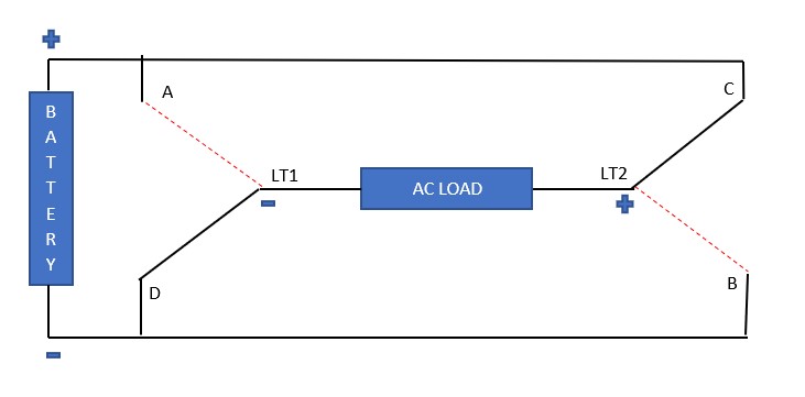
Assume an electrical circuit that works in following manner:

Between load terminals: LT1 and A & D and between LT2 and C & B we have a single pole double throw switch whose operational characteristics could satisfy following operations as described below.
So, for the first half time-period, load should be supplied by +ve voltage, for that:
- A & LT1 and B and LT2 must be shorted.
- D & LT1 and C & LT2 must not conduct and should withstand voltage appearing across them.

Then for a very small-time instant voltage should across load must be zero.
For that:
- A & LT1 and C and LT2 must be shorted or,
- D & LT1 and B and LT2 must be shorted.
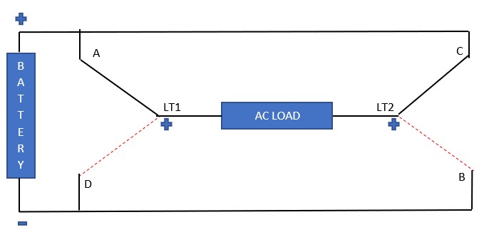
For another half time-period, load should be supplied by -ve voltage, for that:
- D & LT1 and C and LT2 must be shorted
- A & LT1 and B & LT2 must not conduct and should withstand voltage appearing across them.
Now the vague principle of interchanging supply terminals to obtain an AC voltage waveform across a load using a constant voltage battery has become much clearer. Before we go on laying out exact switches required at the load terminals, we have to give a thought on the load current waveform too.
Real-world AC load
When the load is purely resistive- things are simple, the load current will follow the voltage linearly and the direction of current would be from A to B I positive cycle, zero current at t=t/2, and reverse direction in next half cycle.
When you search for switches with such characteristics, then the 21st century Doremon pocket’s hobbyist electronics store (Easy Electronics for SVNITians😅😅😅) will give you a BJT.
With proper base supply, we can obtain the desired characteristics.

But when it comes to real-world, rarely you would find an AC load of unity power factor or we can say purely resistive load in another way.
For non-resistive loads, the current through it and the voltage across the terminals are not linear. For inductive load the current will lag and for capacitive load the current would lead.
Consider a case when the voltage across the load somehow obtained is sinusoidal, which will be obtained in advanced inverter circuits.
The load being inductive, will show the following characteristics.
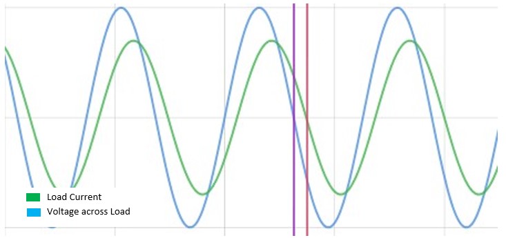
As indicated in the graph at the onset of every -ve half-cycle due to lagging nature, load current won’t reverse its direction similarly for +ve cycle. The above circuitry would reverse the voltage across terminal but it would not be able to sustain the required load current of opposite polarity. This could be easily achieved if we connect a diode to conduct current in short time period at the starting of +ve or-ve voltage waveform.
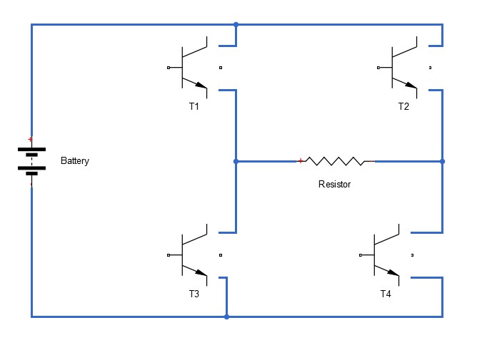
So, the new circuit now becomes:

Let us try to analyze the circuit operating over one complete cycle.

+VE VOLTAGE WAVEFORM:
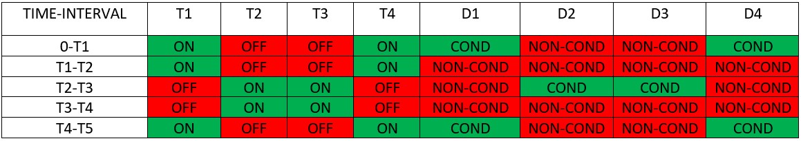
From t = 0 to t = T2, transistors T1 and T4 should be ON and transistors T3 and T4 must be in OFF state.
- t = 0 to t = T1: Current is negative so diode D1 and D4 will conduct.
- t = T1 to t = T2: Current becomes positive hence transistor T1 and T4 conducts.
–VE VOLTAGE WAVEFORM:
From t = T2 to t = T4, transistor T2 and T3 should be ON and transistors T1 and T2 must be in OFF state.
- t = T2 to t = T3: Current is positive so diode D3 and D2 will conduct.
- t = T3 to t = T4: Current becomes negative hence transistor T2 and T3 conducts.
In the following table we have required states of transistor (T1, T2, T3 and T4) to obtain the AC waveform across the load and which diodes are conducting and not-conducting current during the particular time-period.
We can replace the transistor and diode combination by another power electronics device, called power MOSFET. The greatest advantage of using this device is its capability for conduction of current in both directions. Additionally, it gives more power handling and reliable operation. The device is known by name of IRF540.
Internal Schematic Diagram:
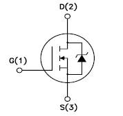
NOTE: The diode shown in the symbol is parasitic. To know more follow the notes or the datasheet of IRF540.
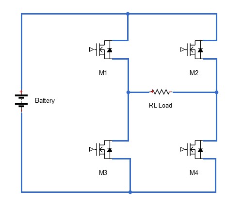
A generalized statement can be made that all the four switches are capable of conducting current in both directions during ON state.
Now let us have a glance on most important parameters of an IRF540 taken for datasheet:
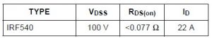
The drain source breakdown voltage is 100V, while most of AC load operate on 230 V RMS voltage i.e. peak value of 325 V. So, this H- bridge configuration is modified for obtaining relatively higher AC peak voltage for low DC battery voltages. This is done by use of a three winding step-up transformer.

In this circuit when M1 is OFF and M2 is ON, the battery injects current to the primary winding (marked 3+) and the voltage appear across the load is +ve. When M1 is ON and M2 is OFF the battery supply the primary winding (marked 2+) and the voltage induces on secondary is -ve (opposite polarity than the first cycle).
Since the MOSFETs can carry bidirectional current through the source and the drain terminal thus this circuit can ve used to power non-linear loads also.
Gate Triggering Circuit
The MOSFETs M1 and M2 should be turned ON and OFF alternatively for 10 ms each for obtaining an AC output voltage of 50 Hz frequency. Numerous IC can be used to design the triggering circuits like IC4047, IC4049, etc.
CONCLUSION
The output voltage wave obtained using the circuit drawn above is a square wave. The Harmonic content would be little more than required for optimal performance.
Using a minor modification to this circuit we can get a modified sine wave.
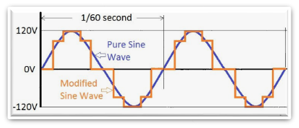
It resembles more closely to pure sine wave hence improved harmonic performance. In the next blog will see how the harmonic performance is computed, measured and improved in inverter circuits, some practical circuits, and much more.
NOTE: Other advanced technique used is PWM (Pulse Width Modulation) technique.
Keep reading, keep learning!
AANTARAK DIVISION
TEAM CEV!!