The following document records the working and insights of a R&D department of an Electrical Instrumentation Manufacturing company, born and bought-up in India in early 1980s, and eventually extending its roots over 70+ countries and sustainably competing in European, Middle-East, Russian, South-East Asian, American and Latin American, and of course Indian Markets.
From advanced Multifunction Meters to legacy Analog Panel Meters, from handheld Multimeters to patented Clamp Meters, from Digital Panel Meters to Temperature Controller, from 10 kV Digital Insulation Testers to 30 kW Solar Inverters, from Current transformers to Genset Controllers, from Power Factor Controller to Power Quality Analyzers, from Batter Chargers to Transducers. From making best-selling products to white labeling for German, American, Polish and UK’s tech giants. From being major supplier of measuring instruments for BHEL, Railways, NTPC, and big and small manufacturing facilities in India to be able to send its devices in SpaceX rockets. This is not a description of a company located in a tech savvy Silicon Valley of most superior nation of world. This is description of just one of many such growing companies in far obscure industrial regions of our Indian sub-continent.
Purpose of this accounting:
To introduce and highlight the major working, thinking and organizing methods of a world that awaits the footsteps of the hopeful graduates out from a relatively cozy boundaries of their college campus.
To produce a testimony of fact that in exact same environment, with exact same people backed by exact same education system, with same so called incompetent Indian working class a company not just leads a product-based market but also beat it’s so called advanced European counter-parts and bring in collective consciousness the descriptions that seriously challenges the conventional assumption of ailing Indian Manufacturing Industry.
To reinforce and bear witness to the fact that the truths and advices we all get to hear from people around us, are not mere variation of pressure in air but if followed with true spirit it literally creates magic and destined to get one to a point of breath taking, heart pounding and soul touching experiences.
Work on Solutions Not on Problems
The key spirit of professional execution is logical optimistic solution finding approach. The problems in front of all of us are all equally compelling and evident, absolutely no doubt in that, resources are limited, time is little, skills are moderate, support is not there, etc. But the point is the R&D mindset will never except them. If resources are not there let’s check-out the savings/loan, if time is not there let’s think about multiplexing, if skill is not there let’s talk to an expert and reach out for help, if support is not there let’s start reading ourselves. With optimism you ask, What exactly is the problem and what needs to be done to counter it, you present yourselves with options select one with maximum logical connections and go do it. If failed, with same optimism you ask that same question again. If you take decision with logical grounded thinking every time you almost hit the solution and in that is the drive for next try.
For example, in our setup, even on just one section of product (let’s say LCD) as many as 24 revisions are made until you uncover the design that has best readability with maximum features considering the space limitations of mechanical housing and even at that point the owner of design will not say no to 25th revision if that’s better than 24th. And here the catch is when someone starts, he can just say no, it is not possible to accommodate all these things on such a small screen, either readability or extra features can be provided, logically that’s correct until someone comes with an optimistic solution finding approach and say let’s first accommodate the unavoidable one, then let’s try some alignments, let’s try some tilts, let’s try some symbols, lets try some overlapping.
An striking example of human genius, the size of screen is less than a little finger of a 5-year old, but is capable to display great deal of data on it.
Doing Detailed and Exhaustive Documentation
It is well accepted and proven thing that if we work well with the documents at office, one is destined to have peaceful life at home, as one does not have to remember any dumb piece of information. You have a flawless access to a time machine kind of thing. A window to look your past works and track back any spurious design back to its origin in a very less time and less frustrating way. Without documentation at any point the situation which appears to perfectly under control can turn into a knife in windpipe type of jacked-up mess. So, maintaining organized folders, Read_Me files with time stamps and quick notes is indispensable.
Organization of Big and Small Things
Organization of assets and swift and flawless access to our resources always help us to do the mundane things in a highly efficient manner. Think about it you are working on your dream project and the time when you got a breakthrough idea in your work you spend next two hours searching the resistor in the plethora of mess you created and never finding it out and in a snip the time you got to try out that idea is gone. Life is fast for all of us, so being ever ready handy with our tools and hacks is always advantageous.
From the 15K Solder gun to a 1 Rupee pin that you may use to temporarily replace the fallen button on your shirt, everything shall be at its designated place. In such degree of organization of everything around us, one feels that readiness and calm to make it through all those massive problems that all of us have.
Organization of assets just not saves time, money and energy but always creates a welcoming environment to get into. And whichever phase of our lives we may be in a high-school student, a college grad or a professional, we can never isolate our work life from the usual personal life that has to go alongside. One may get ill, one may have unsettled debates with parents, one may have problems with food, water, home, discomfort with neighbors, heavy traffic and extra chilled office spaces, etc., all that non-sense that always plagues us, are anyways an inseparable part of life. The things that walk you through is that the highest degree of organization of small things, big assets and of course thoughts in the head.
Choice is at Last Always Ours!
There comes a time when we all get stuck. Some gets resolved after few hours or debugging some stretches over a day, and some extend up to a working week. Rare are those problems that walk along your side for over a month’s duration. If someone is sufficiently in line with ongoing then most of time our divine intuition lets us get to the root of issues in one or two shots.
You found that EEPROM isn’t responding, you take out the datasheet verifies for the connections, check out the supplies found a cap dry, gave a magic touch with your gun and boom the EEPROM rocks.
You found that device is not measuring the current, you took out the circuit and assembly diagrams, verify the components, found all good. Took out the DSO and plug it across the shunts and find that the resistor is burnt. Replace it with new and, boom that’s fixed.
So, every time you take help of logical reasoning of what has to happen to make that happen and that pretty much shows the light. Eliminating one by one the most obvious reasons for the problems. This doesn’t take courage, but the fun starts to fade out as we run out of logical possibilities. It is from here the test of gut starts. When all logical traces have been checked, everything is just as expected to be, except the final output.
In those moments of defeat and dead-ends one gets subjected to an entirely new dimension of thinking which causes a serious humbling effect on professional’s character. When you look back at those time of intense desperations and using your most forceful impacts and still not hitting the thing, the only thing that comes from within is great calm and respect for the nature of reality for being whatever it is.
How would you handle a situation in which accidently a plugin slot gets locked by you in 5 Lakh high priority high-use equipment?
How would you handle the situation in which after months of workings you are just about to shoot for the hand-over of a product to the production and QA teams suddenly reports to you the most dreaded failure of your product, which is expected to drive a long process of iterative tuning?
How would you handle the situation in which you checked, double-checked, triple-checked and still an error made it into your product’s datasheet?
These types of situations lead to increase in speed of blood in veins, ringing in head, and absolute blow to our spirit and whatnot. But even in that chaos things really moves based on the choices we make. One can accept that truth as it is and chose to question what needs to be done and just take that one next step to address it or accept feeling desolated, beaten, and slapped by life like anything.
Choice is ours!
Try out these fundamental methods of organization, thinking and working, and get astounded by the power of it.
Conclusion
The sudden adoption of Western Education System inspired course structuring in Indian Education System has opened up a humongous range of possibilities for young new graduates. Few students find this ideal for their exploring journey, were as many struggle to chose what to pick from the such a large plate of options. The student needs to anticipate the common and advanced skills in their field of liking. Getting the intuition behind the theory, enabling oneself with mathematical tools and methods, getting comfortable with open source environments, getting hands fluent in hardware handling, ability to do documentation and working in an organized and structured manner, all these set of skills proves to be an asset for every team member during the product development.
The IP rights are conserved, names of companies and writer remains anonymous.
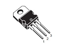
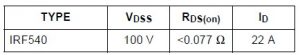
CEV had its first practical hands-on with MOSFETS when we tried to implement a primitive inverter circuit. Device used was IRF540. Back then we didn’t find it so fascinating, considering it just one chisel in our tool-box like resistors, capacitors and inductors, battery, diodes, etc. Only did we moved forward in our lives we realized how one single device characteristic if carefully manipulated can help us to build so many useful stuffs.
If we look at statistics, MOSFETs is most widely manufactured electronic device or component in the entire 200 years of human technical endeavour. The number in fact overshadows all of the other devices lined up altogether. Wikipedia says the total number of MOSFETs manufactured since its invention is order of 10^22. This is just a number we don’t have anything much familiar to correlate and help understand how really big it is.
10000000000000000000000!
Systems like an ordinary radio contain in order of thousands of MOSFETS to provide enough gain to EM waves to finally yield audible audio signals, the smartphone on an average contains in order of 10 Million, an i5 intel core processor contains in order of 1.5 Billion of them, the power supplies for electronic gadgets we use though utilize another variety of MOSFETS called power MOSFETS. The circuitry (power and control) used in handheld devices like trimmer, hair-dryers, toasters, washing machines (automatic), efficient motor assemblies, cars, airplanes, satellites, space shuttles, particle accelerators and what not………., all of them essentially have insane amount of no. of MOSFETs operating in one of its particular desired regions of operating characteristics depending on analog, digital or power device category, very silently and calmly doing its job it is supposed to.
MOSFETS single-handedly forms the backbone of entire analog and digital electronics. Yes, you heard it right, both analog and digital. It lies at the heart of almost all the basic components which are used to build higher-order circuits or devices.
Wait, wait, we promised ourselves to not take anything for granted so when we say analog and digital electronics what do we mean exactly?
Essentially analog and digital are two ways of playing with signals (of voltage or current). Playing here might literally mean fun like playing a song over a speaker, displaying a video on LCD, LED or CRT, talking with loved ones over cellular network, enjoying a live broadcast of a soccer match and capital FM or even as simple as using TV IR remote to frustratingly switch over news channels which spread crap at 9 PM oooooooorrrrrrr playing could also mean stakes as high as using an ECG and other biomedical sensors and instruments to save lives, sending and receiving radio signals of a pilot messages to ATCs, or implementing something as necessary as what we call www.
It is hard to think all of these sharing anything common, right, but in all of the cases we are simply manipulating signals all the time in order to just somehow do what we want using the analog ways or digital ways or most of times both.
Well, it may be hard to think what signal manipulating exactly means here, nor we intend to talk about the grudging details but what we want to first appreciate is the profound immensity and necessity of the things which we are going to talk about.
Again, taking nothing for granted, the first question to address is what exactly signal manipulation would be using analog way or the digital way?
The core requirement of real life the Amplification of signals:
Consider all the different kinds of sensors deployed on field to measure any physical parameter of interest like a temperature sensor in Air conditioners, a metal detector at airports, a stain gauge sensor, an antenna for radio waves detection, a heart-beat or pulse sensor, etc. In all the cases we exploit natural phenomenon to get variation of temperature, strain, EM waves, vibration converted to electrical signals (maybe voltage or current variations). The strength of converted electrical signal is by nature too weak for any purposeful use, like displaying the values of temperature or beats per second on some kind of screen, playing the song received on antenna, etc. The circuits that produce these magical outcomes can’t be driven using signals of such feeble power. We need a man-made device which can significantly boost the signal power.
Graphically. Amplification be like:
2. Filtering is another core requirement of real life:
In the electrical signal at the output of any practical sensors, we have by nature something called a noise. These noises are result of different reasons for different systems. To separate the noise from the useful signal based on the characteristics of systems we use signal manipulation technique called filtering, using something called as filters.
3. Along with these basic kinds of manipulation we have another range of signal manipulation, which essentially helps us to do computation. Like mathematical operations like addition, subtraction, integration, etc. can be achieved using voltage dividers, RC circuits, etc.
In these cases, we by default assumed that signal voltage or current can take infinite number of possible levels in between any two finite levels, between 3 V and 4V, our signal can be 3.11V, 3.111V, 3.1111V, etc.
Why go digital, if we can do it all in analog?
Most of time in digital world first we learn how to do it, then do it and only then we understand why we did it. Digital way of doing things is especially advantageous in doing things described in (3).
Digital way is moving from representing infinite levels signals to no levels between signal levels, only two levels called high and low. This doesn’t make direct intuitive sense unless we study them first.
However, some obvious motivating reasons for moving for digital way is inherent noise immunity, and simplicity.
The digital world has its own kind of signal manipulation requirements like inverter (NOT), adding (AND), orring (OR), etc, in general elements which execute these are called gates.
The layer upon layers upon layers…………
All of this begins by looking at nature. Because we are simply restricted to things, she can provide us, no other choice. Our role is to observe, modify and manipulate whatever she can offer us to make some good use for ourselves.
Resistors, capacitor, inductors, battery, semiconductor switches (Diodes and Transistors) all of this forms the most primitive components which are most basic building blocks. Also, in this category we have devices which exploit natural phenomenon like Photoelectric Effect, Piezoelectric effect, etc. to make sensors like photodiode, strain gauge, etc.
Using these components, we build a little higher order systems, say for example a voltage divider (using battery and resistances), a primitive filter circuits (using resistors, caps and inductors), or maybe most importantly the center of this discussion, an amplifier circuit (resistor, transistor, and battery).
The next order of systems now comprises of these little systems as basic blocks. Like an operational amplifier which uses many amplifier circuits and voltage divider bridges. Something called as gates (NOT, NAND and NOR) are also build using the twisting the same basic amplifier configuration and adding more switches, etc. This layer also set forward two categories we lovingly call analog and digital electronics.
The next layer uses op-amps and gates as their building blocks. For examples in analog world, we can have a comparator, a voltage follower, an integrator, a differentiator, an oscillator, etc. And in digital world we can have what we call combinational logic circuits like flip-flops of varieties D, F, JK, etc.
Things getting interesting right, however still not that useful.
The next layers use these elements as building blocks. Using comparators, integrators etc., we can now start making something like trivial voltage, current and frequency measurement units, we can have active filters, a small power supply, and so on. In digital world the notion of time is introduced by using time signal (clock signals), which is a giant leap.
Now we can have these systems deployed for forming part of even bigger layers. In analog domain we can implement control system feedbacks and jillions other circuits called integrated chips (ICs). Digital world however these days go on building more layers of complexities. The layer of assembly languages, and then higher-level languages like C++ all of them takes off right from here. It becomes so far-reaching that entire branch starts up from here, the CS.
Using these same blocks microprocessors are built, computers also somewhere follow up as we go on and on. EEs have limits on how far they can go, so we stop here, to give the lead for Comps folks.
Personal computers and smartphones are most popular example of highly complex layer upon layers of analog and digital circuits which tends to response to the applied input signal in quite a predictable way. However, the layers of complexity are so magnificent that it is hard to believe that at the core they are made up of fundamental components no different than that of a small TV remote or a decent bread-baking automatic toaster, it is analogous to seeing humans and amoeba under one umbrella, both made of strikingly similar fundamental biological concepts.
One can literally draw the single line connecting these basic elements layer by layer to all sorts of final-end technologies.
Where does MOSFETs fits in all of this?
To have a more insightful view consider these examples:
MOSFETS are fundamental element used in amplifiers.
MOSFETS are fundamental element used in gates.
Amplifiers are themselves basic building blocks of all analog systems. Gates themselves are building block of digital systems.
In this piece, we will see how MOSFETS unanimously able to take fundamentals roles in all the above-mentioned systems.
It all began with Mahammad Attala in Bell laboratories trying to overcome the bottlenecks of BJTs. Namely the higher power dissipation due to base current and hence low packing density, making it impossible to build advanced circuit smaller in size.
MOSFET Physical Construction
Now as engineers we have to be careful in understanding device details as a complete understanding would require backing-up with quantum physics explanations and at least 10 years of dedicated focused study. The key is to carefully listen to physicist and simply ask only for the details which are of our interest.
As far as device is considered, as engineers we need to know is answers to hows and whats only, but strictly no whys.
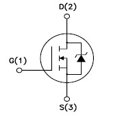
WHAT is a MOSFET?
Image Courtesy Wikipedia
MOSFET is a four-terminal semiconductor device, in which the resistance between two of the terminals is determined by the magnitude of the voltage applied at the remaining two terminals. The range of variation in resistance between two interchangeable terminals called source and drain is very large, extending from few milliohms to 100s of megaohms on relatively small voltage changes at the two terminals called gate and the base (or substrate). For simplicity manufactures internally short the source and the base, it thus becomes a three-terminal device and thus a voltage across gate and source changes the resistance between the source and the drain. This is not all to it, the variation of resistance is not simply linear, it is somewhat weirder, involving several twist and drama of semiconductor physics.
The gate terminal is metal plate separated from the body by an intermediate dielectric layer, SiO2.
The source and drain are two oppositely doped regions as compared to the parent base body of MOSFET.
HOW does it work?
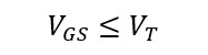
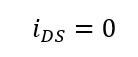
At zero source (or base) to gate voltage, the source and drain terminals are essentially open-circuited, as two p-n junctions appears between them in reverse.
For an n-channel type MOSFET:
As we begin increasing the gate voltage (positive wrt source/base), positive charges begin to accumulate on the metal gate. The corresponding electric field is allowed to penetrate through the intermediate dielectric into the p-type base region between the source and the drain terminal. The exact distribution of field is however currently is beyond our strengths to explain. But the effect is quite intuitive that the minority carrier in p-type will start getting accumulating just below the gate. Not knowing the exact physics but at certain magnitude of voltage level, the devices develop a region so full of electrons that it acts as n-type doped region, and so is called n-channel. This particular voltage is called threshold voltage. The appearance of n-channel effectively results as if the source and drain were connected by a resistance. This 3- D channel’s length and width are inherently fixed by device construction however the depth is determined by the voltage magnitude. The depth is proportional to the excess of the gate voltage above the threshold voltage. This channel indeed truly acts as a resistor, if separation is more the resistance is more (r proportional to length), if the width is more resistance is less (r inversely proportional to the area), and similarly the depth dependence.
Current still won’t flow between the source and drain. If we now also begin increasing the drain voltage wrt source, the ammeter needle comes alive. So common sense says if we go on increasing the DS voltage the current will go increasing linearly, as the channel is an epitome of resistance😂😂😂, but not. The channel depth is proportional to the excess voltage Vgs – Vt. As we go on increasing the drain voltage this excess of voltage mainly responsible for the depth of the channel, constant at the gate end but begins to drop at the drain end. At a certain point, the channel shuts off at the drain end. It is obvious to suspect that current should drop to zero, but instead the current saturates to some constant value, and the phenomenon is catalogued in literature as pinching-off, and device is said to gone in saturation mode.
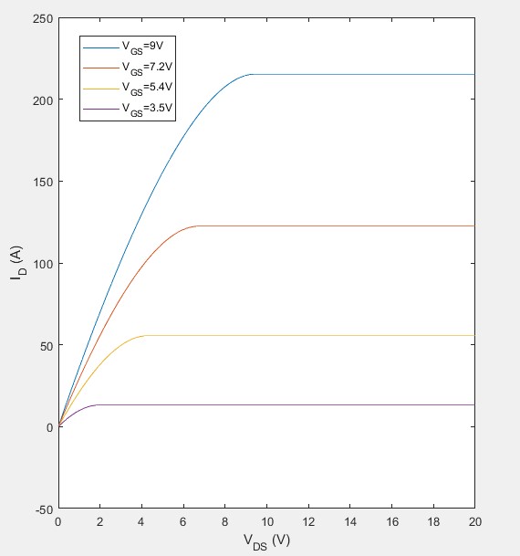
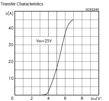
What are the operating characteristics and relevant equations?
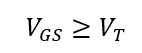
We study the MOSFET characteristics for different values of gate voltage. Until the Vgs is less than Vt the drain current remains zero for all Vds, as if open-circuited. For some Vgs greater than the threshold voltage, we plot Ids vs Vds. At much smaller values of Vds the current increases almost linearly, then due to narrowing of channel at drain end due to increasing Vds, the current saturates to a value at the pinch-off point.
Image Courtesy MATLAB
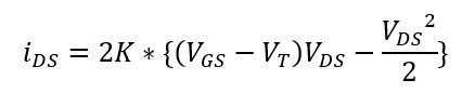
For all:
The drain-source is open-circuit:For all:
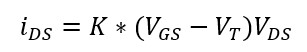
The source-drain current is given by:For small Vds, the square term can be neglected and response is approximately linear:
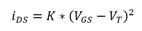
For all Vds ≥ Vgs – Vt, the current saturates at a fixed value, given by substituting Vds = Vgs – Vt:
“What is the distribution of electric field, why at pitching-off it still conducts current, derive the expressions”. All these are extremely interesting questions to take up, but as far as engineering is concerned it won’t help design the circuit any better, so we don’t mind answering them in free time.
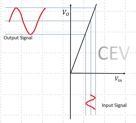
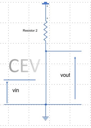
The most repeating circuit pattern of our Electrical lives, we can’t trace anything down to something more fundamental than this. Right here we saw for the first time the gate and the amplifier. Let this pattern dissolve in our blood, imprinted in our DNA, memorized in our brains and printed on walls of our heart. Well, that’s how fundamental it is. 😂😂😂
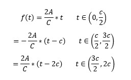
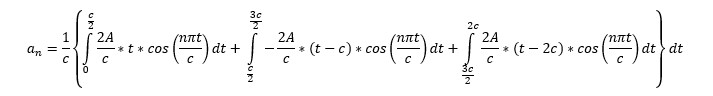
Before directly jumping to equations, let us first build intuition of how this circuit will respond to different applied input, which will allow us to flow through equations smoothly and swiftly.
So, what we need to imagine is the response of the circuit for different applied inputs.
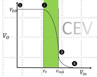
For some applied value of drain voltage Vdd, we begin increasing the gate voltage slowly. As expected, until it reaches the threshold point, drain and source remains open circuited. Current through drain resistor is zero and hence output voltage equals Vdd.
As the threshold potential is reached, the device just develops the so-called n-channel. Notice the current will just begin to flow and DS voltage will thus start dropping. Since the excess voltage is still smaller, and the DS voltage is sufficiently large to drive the MOSFET into the saturation region.
If we still increase the gate voltage then excess gate voltage would be too much for the DS voltage to keep the MOSFET in saturation region. With increasing excess voltage, the channels widen, dropping the resistance, increasing the drain to source current and thus dropping the drain to source voltage, and at one point DS voltage is lower than Vgs – Vt and the MOSFET enters the linear region. (often called triode region)
Notice we understood the operating characteristics is reverse order. To visualize in terms of how the MOSFET operating point moves on the operating characteristics will give more better idea.
At 2, the device just turns on and large value of Vdd immediately drives the MOSFET into saturation up to 3 where the MOS starts entering the triode region. Large dropping the DS, thus the output voltage to a very small value.
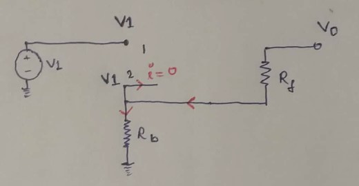
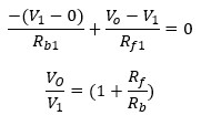
Mathematically:
Applying KVL, we have:
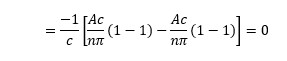
For region 1 to 2:
So,
Hence,
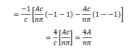
2. For region 2 to 3:
Current saturates at:
Thus, we have:
Parabolic drop confirmed.
3. For region 3 to 4:
Current should be given by equation:
Thus, we have:A rather useless relation. 😀😀😀
MOSFETs as GATES:
We know that any kind of combinational logic can be implemented using three fundamental gates namely NOR, NAND and NOR. How to use this circuit for a NOT operation is quite evident from the transfer curve itself.
For small input voltage range, the output lies in range of some high voltage level, representing digital high logic.
For a range of high input voltage range, the output drops down to a range of small voltage levels, representing a digital low. So, all we need to do is to set Vdd and strictly define the input and voltage range for low and high logic., and we are done, we have got an inverter (NOT).
MOSFETS as Amplifiers
We have seen the requirement of a man-made device called amplifier to obtain a crucial signal manipulation, called signal amplification.
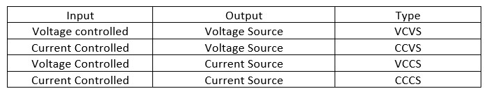
Amplifier in most general way could be called a source of energy which can be controlled by some input. Anyways there may be many more ways to look at amplifier, for example the earlier description of a transfer function block. More specifically this fits better into what we can call a dependent source. Before we understand what is amplifier let us understand what is not an amplifier. So, the element to be first excluded is a potential transformer. Though we can have a voltage amplification (step-up) we also have the currents transformation in inverse proportion so that power remains constant, similarly current transformer, a resistor divider, a boost configuration, etc. in which we have no power gain couldn’t be called amplifier. On the other hand, a MOSFET or a BJT appropriately biased, an op-amps, differential amps, instrumentation amps all are collectively called amplifier. Because we have a power gain at the output port wrt to an input port.
With one port as output and one input and third of course power port, theoretically speaking we can have at max 4 combination. Namely, we can have a current or voltage source at output, and we could have voltage or current control at input.
Any device for purpose of amplification invented in past or been invented or to be invented in future will fall in any one category.
The two-port theory becomes of immense utility, to easily describe different amplifiers in different matrix form, like Z-parameter, Y-parameter, h-parameter and g-parameter. We are constrained to not describe the theory in full detail; however, we will be building insight and motivation to study them.
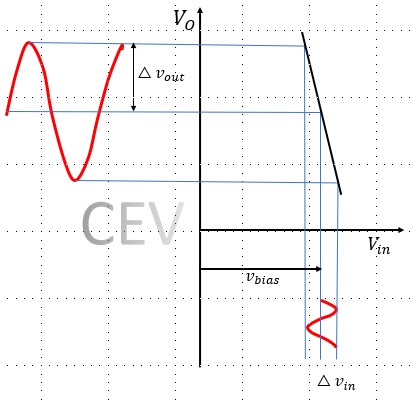
We will use the same trademark configuration to do the amplification too. Isn’t this ground breaking? We had already built fundamental block for digital systems, and now we will again be using the same circuit for amplification which is of course an analog block.
So here it is:
Remember, we didn’t talk about the region between 2 -3 when we studied this circuit acting as an inverter. We strictly worked in 1-2 or 3-4 region only.
The transfer functions in 2-3 region as previously computed is:
Though output voltage is proportional to input voltage, but nowhere close to linear. Remember what we have and compare it with what we wanted:
And here is the greatest revelation as the legends in this field had described for decades.
“The input signal is constrained such that the circuit approximately gives a linear response.”
And the revolutionary constraints are:
Giving a DC level shift, to drive the MOSFET in the saturation region, popularly called biasing voltage, and
if the input signal is small enough the transfer curve is much close to a negative sloped straight line, which is in fact linear amplification.
If we zoom enough, here is how the amplification would look like. Notice inversion is there but a good linear amplification is also achieved.
We can also show that using the equation below that for small changes in input voltage indeed cause a linear change in the output voltage.
For,
We have,
So, we now comprehend the design problem of the amplifier as selection and operation at biasing point to get the best possible linear amplification for a given gain requirement.
And that’s a wrap. From here on we go on learning cascading amplifiers as one unit is not always enough to give desirable gain, which leads us to study the effects of stray and coupling capacitance which becomes especially troublesome when dealing with high-frequency signals, which then leads us to something called differential amplifiers, operational amplifiers, and as already describe we eventually take off from here.
All of this would be no so much use unless we also consider the energy consumption. Why it becomes so important can be understood by walking through some numbers.
Consider an inverter gate is build using the exactly as we have described.
For SMD MOSFETs of today’s technology, typically
K is 1 mA/V^2, Vt =1 V, Vdd we take 5 V (TTL Logic), and let low logic at the output is defined between 0-0.2 V
When gate is OFF, high level at input and low level at output:
Power consumed by circuit is:
For order of 10 million of them:
This very rough approximation of power consumption is not at all pleasant to see for 10 million inverters in days when processors are reaching the range of 4-5 Billion of them.
We would require a dedicated diesel-generator set for one 200-gm machine. Of course, we do something about it, that’s why our laptops could be powered by a 60 W Lithium battery. The solution is quite a creative one. They call it CMOS (Complementary MOS).
In order to have incredibly high resistance, when the gate is off and very small resistance when the gate is on, a PMOS is used to replace the resistor. PMOS transistor has exactly the same operation as NMOS, except it is open-circuited for the high level at input and short-circuited at a low level at the input. Also, Vdd has managed to reduce to 3.3 V to reduce power consumption.
We didn’t learn all of the stuffs by sitting down and just glaring at MOSFETs. The entire credit for vivid imagination and connecting the dots goes to numerous books, all the lecture series, few research papers, beloved Wikipedia and all the awesome discussions we had with our friends.
We are thankful to a Lecture Series on Fundamentals of Digital and Analog Electronics, 6.002 MIT OCW by Prof Anant Aggarwal, two 40 lectures series by NPTEL on Analog Electronics by Prof Radhakrishnan, an introductory lecture series on Semiconductor Physics and Devices by Prof D Das IISc B, Basic Electronics Course by Prof Behzad Razavi of Princeton University. This article is result of rigorous brainstorming of ideas, concepts and insights gained from all the above-mentioned sources and then making our own speculations.
Reading Time: 12minutesOn the occasion of auspicious Diwali, team CEV wonders what could be more relevant and important other than to talk about harmonic resonance!!
Haha, but no kidding!
Since Diwali is a festival of “lights” and in these days harmonics are unanimously voted as the most popular villain in electrical world to turn the “lights” out!
Well if you have been a new reader at CEV, we would like to bring into your notice that our CEV’s Aantarak division have been literally obsessed with power harmonics for a long time now. We had carried out in-depth preliminary literature recon followed by collaborative effort to develop our own harmonic analyzer from scratch. Both can be accessed by following links respectively:
Continuing the same lines, we walked another mile to get ourselves around the harmonic resonance phenomenon, which otherwise has been tagged as seriously spurious.
We really hope to wind up our intuition for harmonics and related phenomenon in this last blog of the series, so we wish to describe it in its full glory. So, you might encounter some repeating themes, apologies for that.
The Crisp
For any domain, having a glance of history really helps in getting a larger picture of the things. Being aware of the historical background greatly aids in understanding the things with continuity and help in extrapolating the ongoings to get some future insights.
So EE folks haven’t begun struggling with harmonics in recent times, infact one can trace it back to early 20th century when power systems were in its earliest phase. Charles Proteus Steinmetz, yes the same engineer who taught the world how to draw the equivalent circuit diagram of induction motor and gave us a handy notation of “j” to simplify our AC calculations had made an excellent introductory paper in harmonics. At that time due to inferior core materials transformers and motors saturated, giving rise to these problems. However, now the problems- harmonics pose remain unchanged but the sources and impact have been magnified manifold.
21st-century power system seems to be literally littered with inky-dinky semiconductor devices which draws currents which are severely offbeat from sinusoidal nature, moreover, the advent of high power electronics has made the situation more vulnerable. Technically these devices/loads are called Non-linear devices/loads, and problem they pose are quite spurious in nature. We know that high-frequency components of these currents called harmonics interact with power system in ways leading to overheating of components, flickering, circuit breaker false trippings, or even causing catastrophic events like a wide-area power outage (aka. Blackouts), as reported by many utilities in recent times across the world.
These harmonics can tune the capacitor banks used for power factor improvement and voltage stability in resonance with the power system components and lead to blowing up of the banks and causing further contingencies, like voltage collapse, etc.
In this blog, a detailed analysis of power factor banks, non-linear loads, resonance phenomenon in RLC, and lastly the resonance in power system due to harmonics is carried out.
One more note, you might be aware of the MATLAB company tagline, it reads “accelerating the pace of science and engineering”, and CEV is really goanna help MATLAB do that here. We will use appropriate MATLAB simulation models to verify the theory and bring home to the readers a sophisticated understanding of the phenomenon.
The Skyrocketing hopes!!!
The flow
Power Factor Capacitor Banks
Thevenin’s Equivalent of Power System
Electrical Resonance in RLCs
Harmonic Resonance with PF Capacitor Banks
Harmonic Resonance, is among the most dreaded phenomenon the power system harmonics are observed to unroll.
ABB, the mega-giant in the power system industry tries to bring on the table the significance of eliminating power harmonics by its product commercial.
Though being regarded as the most suspected reason for unexplained failures of electric utilities the harmonic resonance is a phenomenon that could be explained in a paragraph of no more than 100 words only, you would be able to do it the small kids around you, by the end.
The story begins from the power factor capacitors banks……
You might have appreciated the fact that the use shunt capacitor banks across the electrical motors (lagging loads) can improve the power factor greatly.
The underlying idea is to provide the reactive power locally instead of drawing it from the system thereby reducing the supply current and preventing the elements of the whole power system (from T-lines down to the generators) from overloading.
This concept can be intuitively understood by use of following graphs.
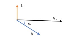
Consider a sinusoidal voltage applied across an inductive load, result is a lagging current.
So, the convention is to simply connect a capacitor bank of required capacitance. Since the capacitor is in parallel so the voltage across it is in phase with load terminal voltage, and the current through it is obviously 90 degrees leading the voltage across it.
The phasor diagram:
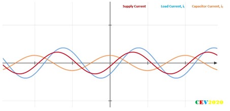
The waveforms are like:
Adding the parallel currents to get the supply current:
So, it could be easily seen that the peak of the resultant current has been reduced, at the same time the power factor angle is also reduced hence power factor improved!!
This same result can be concluded by simply adding the current vectors mathematically.
So, what exactly is happening here?
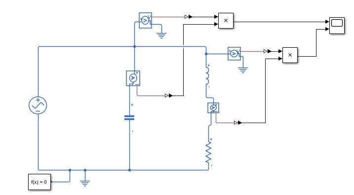
The picture becomes crystal clearer if we try to simulate an RL load with shunt capacitor and visualize the instantaneous power consumed by each element.
By putting appropriate parameter values, it could be seen that when inductor is absorbing power the capacitor is releasing its stored power, and when the inductor is releasing the stored inductive power in its magnetic field, the capacitor is absorbing it in its electric field. It is this inductive and capacitive power, are collectively called reactive power, which just flows in the system but never manifests itself as real power, rather just oscillates. If this power exchange becomes equal then no net reactive power is drawn from the source.
So final result is “significantly reduced net reactive power drawn from the source and so is the supply current”.
Question: Do you think that the capacitor in ceiling fans of households serves the purpose of PF improvement?
Now to analyze the effect of shunt capacitor for non-linear loads, i.e. loads that produce harmonics, we have to follow a different approach, a completely different line of attack.
However, the theory we just saw is equally true, but as far as harmonics are concerned, we are more interested in first understanding the frequency response, rather than power calculation.
Some of the most basic and prevalent techniques used everywhere and all the time in power system analysis are first required to be grasped before we try to understand what happens for non-linear loads.
The concept of Thevenin’s equivalent;
The concept of current injecting vector
The concept of superposition
Thevenin’s Equivalent of Power System
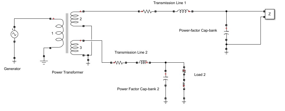
Consider this point of view, the two-terminal is supplying a single-phase non-linear load, also conventionally a power capacitor is applied in parallel to supply reactive power locally. The black box here is an abstraction of all the distribution and transmission transformers, transmission lines and the generators and whatnot, all working in synchronism.
So, the Thevenin theorem says that the black box can be represented by an equivalent emf source and an equivalent impedance in series, called Thevenin’s voltage and Thevenin’s impedance respectively.
The Thevenin voltage is simply the open circuit terminal voltage.
And the Thevenin impedance is the impedance seen by the load given all the voltage and current sources are deactivated.
Once the Vth and Zth are known, to know the impact of connecting a load impedance to already loaded grid we don’t go on solving whole vast electric mesh again. A revolutionary French electrical engineer LC Thevenin in 1880s came up with a revolutionary method to enormously simplify the large electrical circuit.
Find Vth and Zth. Now turn off all the sources, connect the load wherever required, excite the point with the negative Vth, find the drop and add the drops algebraically to already existing system. This is applicable only for linear system by virtue of superposition theorem. This line of attack is chosen when the load impedance is center point (i.e. load impedance is known). This is quite a popular technique and is implied to calculate the impact of loading on different buses of system, fault analysis for a known value of fault impedance, etc.
Now, if impact of a given load current is point of attention (rather than the load impedance) then we use slightly different approach. We turn off the source and inject an equal load current at the point of connection of load, find drops at different nodes and again added algebraically to the existing system.
Now in this case of harmonic resonance study, notice we are utterly concerned with the load current. Our prime moto is to see the impact of a given non-sinusoidal load current on the system.
Here it is important to reflect to one important fact. Our power system is built up of thousands of different kinds of elements, the generators synchronous and asynchronous IMs, the transformers, T-lines, cables, a huge variety of loads, yet all of them can be modelled as a combination of just three fundamental elements, resistance, inductance and capacitance.
Q. How would you modify the Thevenin equivalent if the power systems have power electronic components?
So, it is all those little-tiny things learnt in early engineering classes of circuit theory comes back to manifest in harmonic resonance and other complicated higher phenomenon. Here we realise that solving the RLC circuit is not dull, unless we know how far-reaching are the meaning of those Rs, Ls and Cs in a practical applications.
But all of these theories are strictly applicable to a linear system.
Think for a second how to manipulate the tools for the non-linear currents.
So, lets revisit our aim, our aim is to find the impact of non-sinusoids, that means we are trying to see the response of system subjected to different frequencies. Now this leading us to a completely different space. Did you remember a phenomenon related when we check the response of a system to input of different frequencies?
You guessed it right, the series and parallel RESONANCE!!!!!
Moreover, we are finding the frequency response and by the time we have completed the course in control engineering, frequency response characteristics of any system almost become synonymous to bode plot.
It becomes as good as people screaming to you to “draw frequency characteristics” and you literally hear “draw plot bode-plot”!
And why not, after all, bode plot is a plot of the logarithm of magnitude of steady state output to input for different frequency of sinusoidal input excitations.
Electrical Resonance in RLCs
Resonance in series circuit can be identified as a phenomenon in which for a given magnitude of sinusoidal voltage source, current through the branch reaches maximum at some angular frequency of voltage source.
Here is bode-plot for the system considering the voltage signals as input and the current in the branch as output:
The plot indicates that at a certain frequency of voltage excitation the current through the circuit reaches its maximum value.
Similarly, parallel resonance can be identified as a phenomenon in which for a given magnitude of sinusoidal current source, the voltage across the branch reaches a maximum at some angular frequency of the current source.
Reflecting on these two base-statement rest all of the conditions of resonance can be deduced.
So here is a bode-plot of parallel RLC circuit taking voltage across the elements as output and total current as input.
In this case the voltage reaches a peak corresponding to the resonant frequency.
Harmonic Resonance with PF Capacitor Banks
We have built all the necessary parts and now it’s the time to put all the parts together to see the larger picture, and really wind-up our intuition around the harmonic resonance. We started with this not so technical diagram:
Reflect back and finally, we have:
It is now quite evident that parallel resonance is seen where parallel elements are excited by a range of angular frequency currents. These parallel elements in a power system are formed by the PF capacitors and the Thevenin’s equivalent at the node. The non-linear load is going to act as a source of different angular frequency current source. So, if the non-linear loads have the harmonic component which has a frequency as the natural frequency of the RLC then a parallel resonance is unavoidable fate.
And this is in-short the hack of harmonic resonance in power systems.
Wouldn’t it be delightful to let a kid know about this?
A Practical Approach
How to obtain the harmonic spectrum of a non-linear load?
Matlab gives you an elegant way forward, use a spectrum analyzer (in a correct configuration)
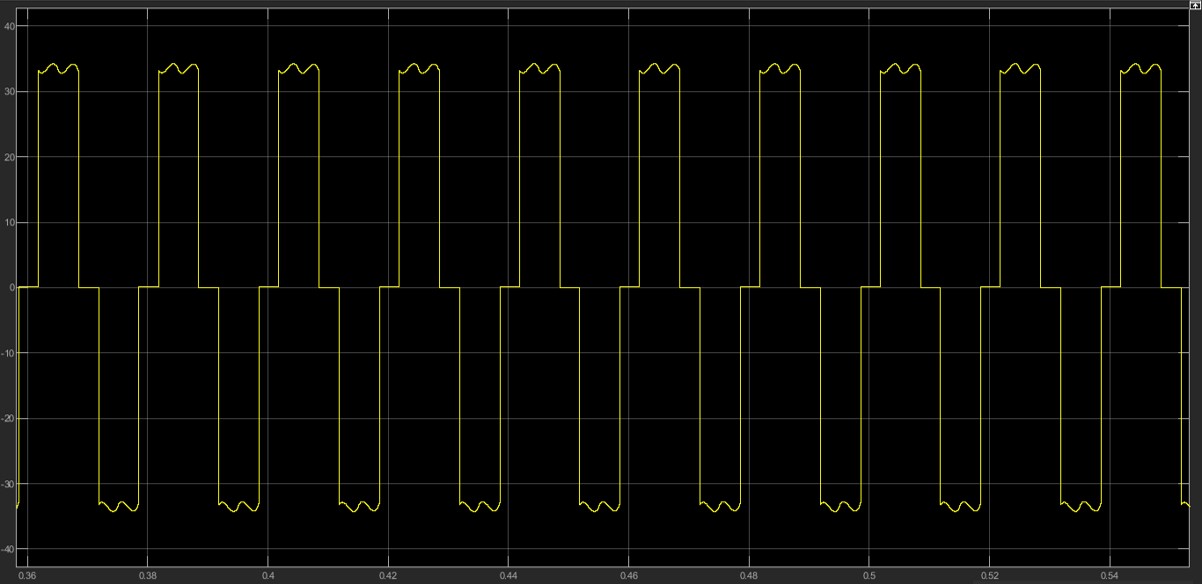
A sample case of a popular non-linear load, a three-phase rectifier:
A severely off-beat source current:
Here is what its harmonic spectrum looks like:
NOTE: 6-Pulse rectifiers have a current THD of 26% and significant harmonics are 5th (250 Hz), 7th (350 Hz) and 11th.
How to obtain the Thevenin equivalent of a power system?
The answer remains the same the MATLAB provides an elegant way to do it.
Using an impedance measurement block:
What you get is:
If you are observant enough, these plots contain all of the data that we are searching to be able to predict a harmonic resonance in capacitor bank across the non-linear load.
Well, we will leave it to you to build and run the models for yourself because we don’t want to steal your pride of finding and fixing things out on your own, so good-luck…………
However, in the end, we will be kind enough to atleast make a conclusion:
The conclusion reached is, when the non-linear load has a current component of frequency close or equal to the natural frequency, the system goes in parallel resonance i.e. system impedance is highest. For a given current value at the highest impedance would clearly result in the highest voltage drop across the capacitor, hence maximum current through it (notice the value of capacitive reactance decrease at higher frequencies).
The capacitor is immediately blown, as a result, the reactive power is drawn from the supply leading to increased current, thereby blowing the main fuse also. And the last sad thing to be noted is that if the capacitor comes out to be a utility capacitor and non-linear load is quite heavy then a blackout in the area is unavoidable destiny.
What is even more surprising is that current harmonics produce parallel resonance that we just saw, however, if there are harmonics presence in voltage waveform then series resonance could also occur in a dramatic way. Causing the collapse of a perfectly healthy bus due to non-linear load at another bus. One can also work-out its details on our own!
We hope we have inspired you enough to get yourself easy with the extremely useful tools in Electrical engineering, the massive MatLab and the sweet Scilab, and hope that CEV team effort boosts you a step towards your holy dream vision for the world!!
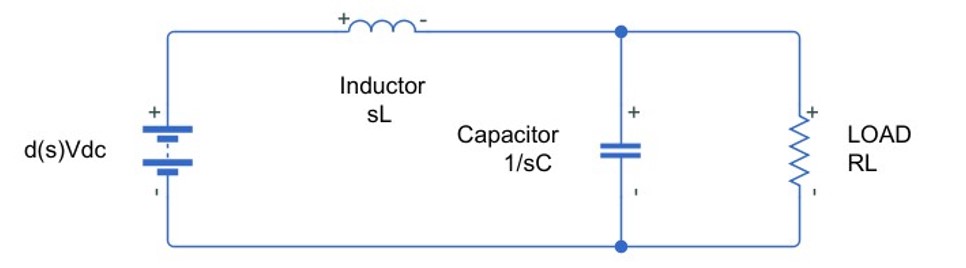
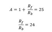
A controlled buck converter finds its application in innumerous platforms. It elegantly executes the mobile fast charging algorithm, MPPT algorithm in some Solar modules, robotics, etc. with optimal desired performance. It is elementary power converter, used as a power source for other electronic equipments like microprocessors, relays, etc.
One can jokingly say it the 1:1 auto-transformer of DC electricity world.
Buck converters which are also known as step-down choppers, are much ubiquitous hence it becomes very handy to have a design scheme, tested procedures and simulation models to fastly and accurately build a ready to deploy DC Buck converter. We will not describe in great depths the working as the principle of operation can be found in any standard power converter textbook, however, in this blog we wish to present a step by step guide to design a buck by taking into account all important practical considerations.
General Schematics
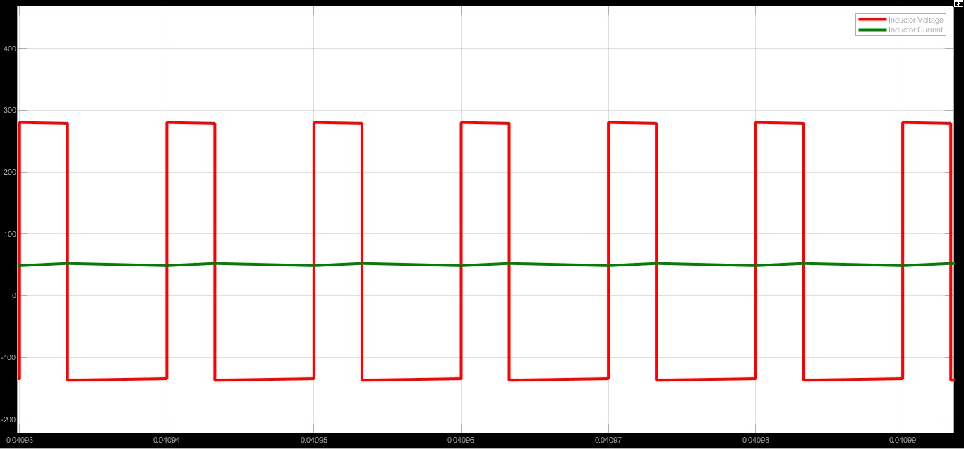
The circuit operation can easily be understood by sketching the waveforms in two states, i.e. when the semiconductor switch is triggered and when it is not triggered.
ON-STATE: Inductor current rises linearly with time as voltage source get directly applied across the inductor and load.
OFF-STATE: Inductor current decreases linearly as the circuit gets short-circuited by the forward-biased diode, which allows for current free-wheeling.
The average voltage applied is a function of time for which the semi-conductor is turned on and turned off, which is indicative of the duty cycle of the pulse generator.
Specifications
The first thing we require is all the desired ratings and performance of the buck converter. These specifications ultimately determine the device parameters, which will give the desired operation. Consider the sample case in which we are operating a constant power load with a variable input DC voltage source, for example a solar module.
Ratings:
Input: 150 V- 400 V
Output: 120 V
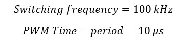
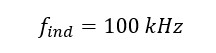
Switching Frequency: 100 kHz (typical for choppers)
Load current: 50 A
Performance Parameters:
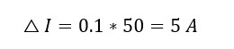
Ripple (P-P) in load current: 10%
Ripple (P-P) in load voltage: 5%
Max Load Power support: 25%
Max Voltage drop during support: 10%
Backup duration: 10 ms
Keeping in mind these desired performance parameters the ratings of the various elements will be decided.
Circuit Element Rating Calculations
Inductor
The value of Inductor determines the ripple in the load current. Having large ripples in load causes poor performance of DC load, like lights will flicker, DC fans will produce pulsating torque and noise, etc.
Since varying the duty-cycle will result in different turn-on and turn-off time thus causing varying ripples. All we have to do is to do a trial and error procedure to find the value of L to get ripple below permissible limits under all possible cases:
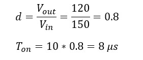
Test case 1: Vin = 150 V; Vout = 120 V
For peak to peak ripple current of 10%:
Now inductor equation during on-time is:
From circuit:
*Assuming load voltage remains almost constant during the entire cycle
So,
Now here comes very crucial part. The theoretical value of inductor has been calculated, but the important things is, in the real environment we always need to overrated our circuit elements to accommodate the uncertainty of the real world. If we are designing a commercial product there is a very tight margin for these over-ratings. That’s why all the gadgets are always rated to operate in a specified environments, like temperature, moisture, etc.
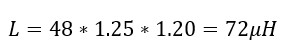
It is good practice to keep a safety factor of 25% for operating temperature changes and 20% for derating of inductor coil over time:
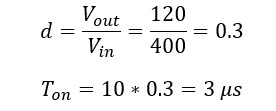
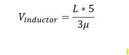
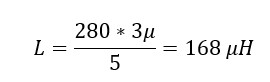
Extreme Test case 2: Vin = 400 V; Vout = 120 V **Worst case calc
For peak to peak ripple current of 10%:
Now inductor equation during on time is:
From circuit:
*Assuming load voltage remains almost constant during the entire cycle
So,
Again, keeping a safety factor of 25 % for operating temperature changes and 20% for derating over time:
Now since worst-case requirement doesn’t meet previous case value thus the inductor value should be updated to at least 252 uH.
We must also verify the ripple current requirement at met for input voltage in between 150 V and 400 V:
Random Test case 3: Vin = 250 V; Vout = 120 V
Hence verified!
Now max current through inductor:
Also,
So finally, inductor ratings are:
Parameter met:
Ripple current is less than 10% for all cases.
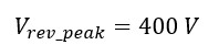
Semiconductor Switch
Peak Reverse voltage occurs under off-time:
Considering safety factor of 30%:
Peak current would be same as inductor current, and taking safety factor of 25% and 30% for spikes due to stray inductance and temperature rise;
So, the semiconductor switch ratings are:
*RdsON should be as low as possible.
*Now since the reverse peak voltage is less than 600 V so a MOSFET can be employed, however if gating loss has also to be considered than IGBTs would be preferable.
Diode
Diode will also be subjected to same voltage and current ratings as that of the MOSFET.
*In addition, care must be taken to select a diode will high frequency operating capabilities in order of 100 kHz.
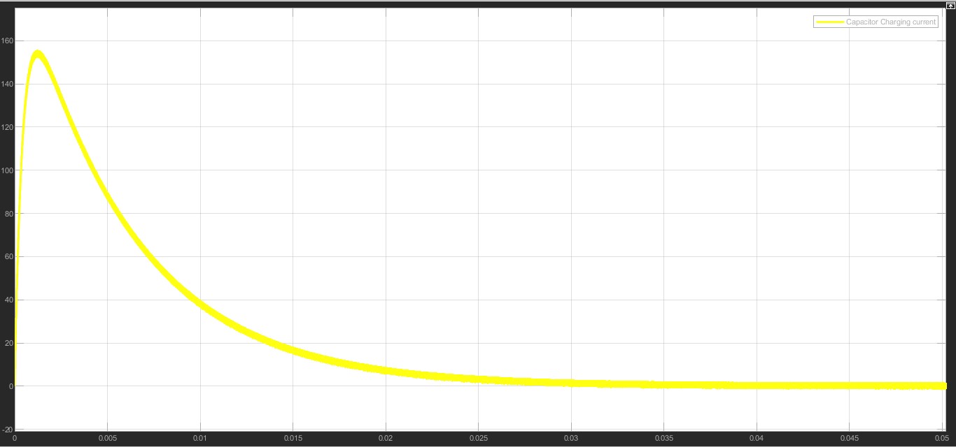
Capacitor
The high-frequency ripple present in the inductor current will be bypassed by the capacitor, as its impedance varies inversely with frequency. However, in an ideal capacitor, there is always some series resistance with leads to ripples in voltage across the C terminal, inturn the load terminal.
Effective Series Resistance (ESR) Ratings:
A ripple of less than 2% is desired in output voltage, so:
Since ripple in load voltage is largely caused by the series resistance,
Parameter met:
Load Ripple voltage of less than 2% is obtained for all cases since 5A is the maximum ripple in the current.
Moreover, this charged capacitor discharges to meet the load current for a small duration when supply is lost or small increase in load. This same principle is applied in many electronic gadgets like PC, laptops, etc to bridge the power loss during switching from mains supply to back-up power.
2. Capacitance value:
For a load change of 25% a corresponding load voltage dip of 10% and a backup time of 10 ms is desired.
10% Dip in voltage:
25% change in load is:
This power should be supplied by the capacitor and thus will discharge it:
Making critical approximations, which we all engineers so good at:
Capacitor voltage with 30% safety factor:
So:
Parameter met:
The load voltage drop of less than 10% is obtained for 10 msec for a load increase of 25%.
Simulations
**MATLAB MODEL
Displays show the result for 400V input, notice 120V output and 50 A load current.
Now comes the most elegant part of designing a buck converter, modelling a buck to understand and predict the performance in a closed-loop operation.
Like any linear control system, we first need to identify the input and the output. Here we have reduced the buck converter to a simple RLC circuit to check the response of the system for various input of duty cycle:
The transfer function model obtained for this open-loop system is as follows:
Where:
Now as per one’s convenience we can either go with root-locus analysis or with the frequency domain analysis.
We know from control theory that by obtaining the bode-plot of an open-loop system we can say a lot about the closed-loop operation of the system. We can comment on the stability, relative stability as well as with little speculations we can also comment on the transient response!!
We might have dived in depths of Control Theory, but we restrict ourself to buck only. Probably, we will find some other fine day to do that.
Obtaining the bode-plot for above open-loop transfer function by running the following code in SCILAB:
From bode-plot it can be directly concluded that the close loop system will be unstable as the phase cross over frequency is less than the gain cross-over frequency.
By the conventional steps, we need to first use a lag compensator to make gain-cross over frequency less than the phase cross-over frequency.
Adding a lag-compensator around the gain crossover frequency of around 2000 Hz.
Adding lag compensation at around 2000 Hz is given by:
Bode-plot for the lag compensated system:
It is evident that now the close-loop system of this open system will be stable but the margin of stability is less.
So, using a lead compensator to provide the required phase margin at the gain cross over frequency, i.e. around 2000 kHz.
TF for required lead compensation should be:
A well-compensated and stable system:
*If desired more lead compensation can be provided according to the design specs.
The final open-loop gain becomes (assuming unity feedback system):
Now op-amp can be used to make these lag and lead compensators, and using analog electronics duty ratio generation could also be done. CEV ask for apologies to not do that today.
The Last Words
Team CEV’s purpose of posting technical blogs is to help out some of the folks who have been completely or partially saddened by the conventional ways of teaching and have been extremely demotivated to keep their interest in these kinds of stuff which is otherwise so rich and interesting.
We are aware that the system has failed us to boost and strengthen our interest in the subjects. 1/7 th of humanity shall not be devoid of fun and joy of falling in love with the subjects, by no fault of their own.
This is simply not acceptable to CEV.
We are not here to just do casual criticizing about the things rather we understand the severity of the situation and quiet boldly take the ownership to undo the damage, even by a fraction of %.
We believe that people in light of their own personal insights can put out things is much appealing and fascinating way, unlike the usual exam-focused, dull and dead description of things. We intend to rekindle the fire of curiosity and interest and help keep the learning spirits of our generation of student community real-high.
“Do you have the courage to make every single possible mistake, before you get it all-right?”
-Albert Einstein
**Featured image courtesy: Internet
THE PROJECT IN SHORT: What this is about?
The importance of analyzing harmonics has been enough stressed upon in the previous blog, Pollution in Power Systems.
So, we set out to design a system for real-time monitoring of voltage and current waveforms associated with a typical non-linear load. Our aim was “to obtain the shape of waveforms plus apply some mathematical rigour to get the harmonic spectrum of the waveforms”.
THE IDEA: How it works?
Clearly, real-time capabilities of any system are analogous to deployment of intelligent microcontrollers to perform the tasks and since this system also demanded some effective visualization setup, so we linked the microcontroller with the desktop (interfacing aided by MATLAB). Together with MATLAB, we established a GUI platform to interact with user to get the required results:
The shape of waveforms and defined parameters readings,
Harmonic spectrum in the frequency domain.
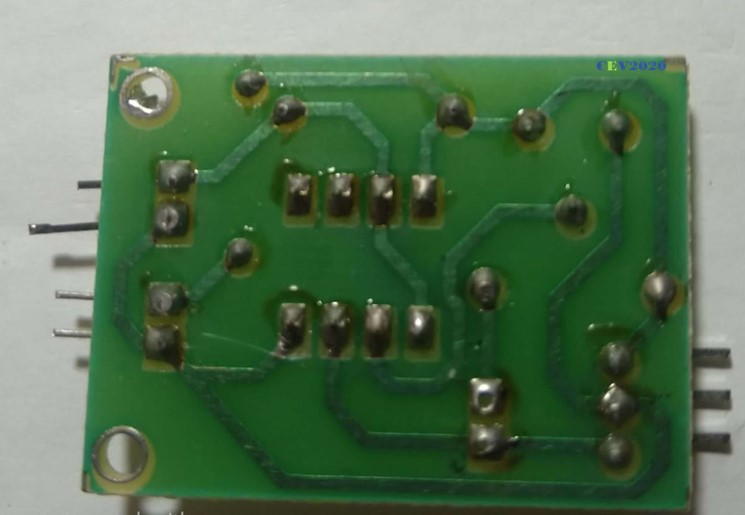
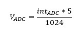
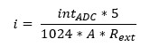
The voltage and current signal are first appropriately sampled by different resistor configurations, these samples are then conditioned by analog industry’s workhorses, the op-amps, and are fed into the ADC of microcontroller (Arduino UNO) for digital discretization. These digital values are accessed by MatLab to apply mathematical techniques according to commands entered by user at the GUI to finally produce required outcome on screen of PC.
ARDUINO and MATLAB INTERFACING: Boosting the Computation
Arduino UNO is 32K flash memory and 2K SRAM microcontroller which sets limit to the functionality of a larger system to some extent. Interfacing the microcontroller with a PC not only allows increased computational capability but more importantly it serves with an effective visual tool of screen to display the waveforms of the quantities graphically, import data and save for future reference and so on.
TWO WAYS TO WORK: Simulink and the .m
The interfacing can be done via two modes, one is directly building simulation models in Simulink by using blocks from the Arduino library and second is to write scripts (code in .m file) in MatLab by including a specific set of libraries for given Arduino devices (UNO, NANO, etc.).
Only the global variable “arduino” needs to be declared in the program and rest codes are as usual and normal. We have used the second method as it was more suitable for the type of mathematical operation we wanted to perform.
NOTE:
The first method could also be utilised by executing the required mathematical operation using available blocks in the library.
Both of these methods of interfacing require addition of two different libraries.
THE GUI: User friendly
Using Arduino interfaced with PC also gives another advantage of user-interactive analyzer. Sometimes the visual graphics of waveform distortion is important and sometimes the information in frequency domain is of utmost concern. Using a GUI platform provided by MatLab, to give the option to user to select his choice adds greatly to the flexibility of analyzer.
The GUI platform appears like this upon running the program.
MatLab gives you a very user-friendly environment to build such useful GUI. Type guide in command window select the blank GUI and you are ready to go.
Moreover, you can follow this short 8 minutes tutorial for the introduction, by official MatLab YouTube channel:
Once GUI is designed and saved, a corresponding m-file is automatically generated by the MatLab. This m-file contains the well-structured codes as well as illustrative comments to show how to program further. The GUI is now ready to be impregnated with the pumping heart of the project, the real codes.
COLLECTING DATA
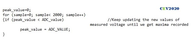
The very first task is to start collecting data-points flushing-in from the ADC of the microcontroller and save it in an array for future reproduction in the program. This should be executed upon the user pressing the START button at the GUI.
Algorithm:
Since we have shifted our whole signal waveform by 2.5 V so we have to continuously check for 127 level which is actually the zero-crossing point, and then only start collecting data.
Code:
% --- Executes on button press in start.
function start_Callback(hObject, eventdata, handles)
% hObject    handle to start (see GCBO)
% eventdata  reserved - to be defined in a future version of MATLAB
% handles    structure with handles and user data (see GUIDATA)
V = zeros(1,201);
time = zeros(1,201);
vstart = 0;
while(vstart == 0)
    value = readVoltage(ard ,'A1');
    if(value > 124 && value < 130)
        vstart = 1;
    end
end
for n = 1:1:201
    value = readVoltage(ard ,'A1');
    value = value – 127;
    V(n) = value;
    time(n) = (n-1)*0.0001;
end
DISPLAYING WAVEFORM
The data-points saved in the array now required to be produced and that too in a way which makes sense to the user, i.e. the graphical plotting.
Algorithm: ISSUES STILL UNRESOLVED!!!
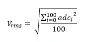
HARMONIC ANALYSIS
As mentioned previously we aimed to obtain the frequency domain analysis for the waveform of concern. The previous blog was presented with insights of mathematical formulation required to do so.
Algorithm: Refer to blog Pollution in power systems
Codes:
% --- Executes on button press in frequencydomain.
function frequencydomain_Callback(hObject, eventdata, handles)
% hObject    handle to frequencydomain (see GCBO)
% eventdata  reserved - to be defined in a future version of MATLAB
% handles    structure with handles and user data (see GUIDATA)
%Ns=no of samples
%a= coeffecient of cosine terms
%b =coefficient of sine terms
%A = coefficient of harmonic terms
%ph=phase angle of harmonic terms wrt fundamental
%a0
sum=0;
n=9   %no of harmonics required
[r,Ns]=size(V);
for i=1:1:Ns
   sum=sum+V(i);
   Adc=sum/Ns;
end
for i=1:1:n
    for j=1:1:Ns
       M(i,j)=V(j)*cos(2*pi*(j-1)*i/Ns);%matrix M has order of n*(Ns)
    end
end
for i=1:1:n
    for j=1:1:Ns
        if j==1 || j==Ns
            sum= sum+M(i,j);
        elseif mod((j-1),3)==0
            sum=sum+ 2*M(i,j);
        else
            sum=sum+3*M(i,j);
        end
    end
   a(i)= 3/4*sum/Ns;
   sum=0;
end
for i=1:1:n
    for j=1:1:Ns
       N(i,j)=V(j)*sin(2*pi*(j-1)*i/Ns);%matrix M has order of n*(Ns+1)
    end
end
for i=1:1:n
    for j=1:1:Ns
        if j==1 || j==Ns
            sum= sum+N(i,j);
        elseif mod((j-1),3)==0
            sum=sum+ 2*N(i,j);
         else
            sum=sum+3*N(i,j);
        end
    end
    b(i)= 3/4*sum/Ns;
    sum=0;
end
for i=1:1:n
    A(i)=sqrt(a(i)^2+b(i)^2);
end
for i=1:1:n
    ph=-atan(b(i)/a(i));
end
figure;
 x = 1:1:n;
 hold on;
 datacursormode on;
 grid on;
 stem(x,A,'filled');
 xlabel('nth harmonic');
 ylabel('amplitude');
CIRCUIT DESIGNING: The Analog Part
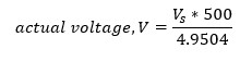
The section appears quite late in this documentation but ironically this is the first stage of the system. As we have seen in the power module the constraints on signal input to ADC of microcontroller:
Peak to peak signal magnitude should be within 5V.
Voltage Signal must be always positive wrt to the reference.
To meet the first part, we used a step-down transformer and a voltage divider resistance branch of required values to get a peak to peak sinusoidal voltage waveform of 5V.
Now current and voltage waveforms obviously would become negative wrt to reference in AC systems.
Think for a second, how to shift this whole cycle above the x-axis.
To achieve this second part, we used an op-amp in clamping configuration to obtain a voltage clamping circuit. We selected op-amp due to their several great operational qualities, like accuracy and simplicity.
Voltage clamping using op-amps:
The circuit overall layout:
IMP NOTE: While taking signals from a voltage divider always keep in mind that no current is drawn from the point of sampling, as it will disturb the effective resistance branch and hence required voltage division won’t be obtained. Always use an op-amp in voltage follower configuration to take samples from the voltage divider.
Now it is always preferable to first model and simulate your circuit and confirming the results to check for any potentially fatal loopholes. It helps save time to correct the errors and saves elements from blowing up during testing.
Modelling and simulation become of great importance for larger and relatively complicated systems, like alternators, transmission lines, other power systems, where you simply cannot afford hit and trial methods to rectify issues in systems. Hence, having an upper hand in this skill of modelling and simulating is of great importance in engineering.
For an analog system, like this, MatLab is perfect. (We found Proteus not showing correct results, however, it is best suited for the simulating microcontrollers-based circuits).
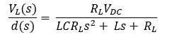
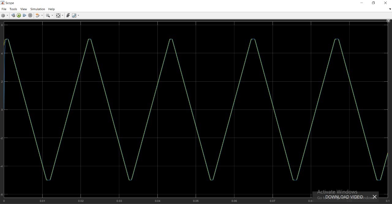
Simulation results confirm a 5V peak to peak signal clamped at 2.5 V.
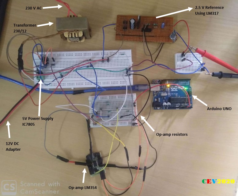
The real circuit under test:
Case of Emergency:
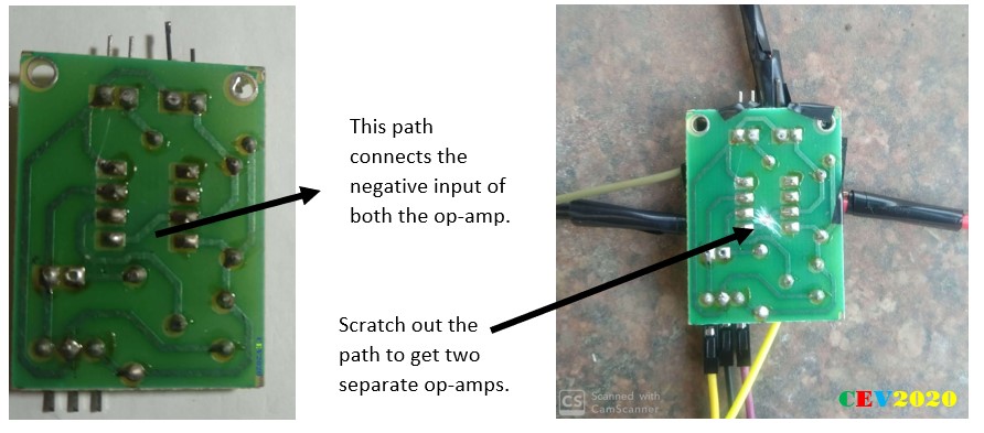
Sometimes we find ourselves in desperate need of some IC and we didn’t get it. At that time our ability to observe might help us get some. In our surroundings, we are littered with IC of all types, and op-amp is one of the most common. Sensors of all types use an op-amp to amplify signals to required values. These IC fixed on the chip can be extracted by de-soldering using solder iron. If that doesn’t seem possible use something that gets you the results. Like in power module project we manage to get three terminals of the one op-amp from IR sensor chip, here we required two op-amps.
First, trace the circuit diagram of the chip by referring the terminals from the datasheet, you can cross-check all connections by using the multimeter in connectivity-check mode. Then use all sorts of techniques too somehow obtain the desired connections.
Reference Voltages
Many times, in circuits different levels of reference voltages are required like 3.3V, 4.5V etc. here we require 2.5 V.
One can-built reference voltage using:
resistance voltage dividers (with op-amp in voltage follower configuration),
we can directly use an op-amp to give required gain to any source voltage level,
the variable reference voltage can be obtained by the variable voltage supply, we built-in rectifier project using the LM317.
WAVEFORM GENERATION
For program testing, we required different typical waveforms like square and triangle wave. These types of waveforms can be obtained in two different ways: the analog way and the digital way.
The Analog Way
Op-amps again come for our rescue. Op-amps when accompanied by resistors, capacitors and inductor seemingly provide all sorts of functionalities in analog domain like summing, subtracting, integrating, differentiating, voltage source, current source, level shifting, etc.
Using a Texas Instrument’s handbook on Op-amp, we obtained the circuit for triangle wave generation as below:
The Digital Way
Another interesting way to obtain all sorts of desired waveforms is by harnessing microcontroller. One can vary the voltage levels, frequency and other waveform parameters directly in the code.
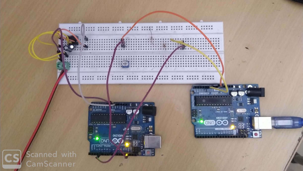
Here we utilised two Arduinos, one stand-alone Arduino 1 which is programmed to generate square wave and another Arduino 2 interfaced with Matlab to check the results.
Now already stated the importance of simulation.
So, here for the simulation of Arduino we used “Proteus 8”.
The code is written in Arduino App, compiled and HEX code is burnt in the model in proteus.
The real-circuit:
The results displayed by the Matlab:
NOTE:
To generate different waveforms other than square-type one thing that has to consider is the PWM mode of operation of Digital pins. The 13 digital pins on Arduino generates PWM.
At 100% duty cycle 5 V is generated at the output terminal.
digitalWrite (PIN, HIGH):This code line generates a PWM of 100% DT whose DC value is 5V.
So, by changing the duty cycle of PWM we can obtain any level between 0-5 V.
analogWrite (PIN, Duty_Ratio):this code line generates a PWM of any duty-ratio (0-100%) hence any desired value of voltage level on a digital pin.
For example:
analogWrite (2, 127):gives an output of 2.5 V at D-pin 2.
Moreover, timer functionalities can be utilized for a triangle wave generation.
THE RESULTS
It is very saddening for us to not able to finally check our results and terminate the project at 75% completion due to unavoidable instances created by this COVID thing.
THE RESOURCES: How you can do it too?
List of the important resources referred in this project:
Op-amp cook book: Handbook of Op-amp application, Texas Instruments
THE CONCLUSIONS: Very Important take-away
“TEAMWORK Works”
If we (you and us) desire to take-on venture into the unknown, something never done before and planning to do it all alone, trust our words failure is sure. It gets tough when we get stuck somewhere and it gets tougher only.
We all have to find the people who have the same vision as ours, share some interests and with whom we love work alongside. We all have compulsorily to be a part of a team, otherwise life won’t be easy nor pleasing. There is a great possibility of coming out a winner if we get into it as a team, even if the team fails, we don’t come out frustrated at least.
Each member brings with themselves their own special individual talent to contribute to the common aim. The ability to write codes, the ability to do the math, the ability to simulate, the ability to interpret results, the ability to work on theory and work on intuition, etc. A good teamwork is the recipe to build great things that work.
So, we conclude from the project that teamwork was the most crucial reason for the 75% completion of this venture, and we look forward to make it 100% asap.
Harmonics Generation: Typical Sources of harmonics
Effects
**Featured image courtesy: Internet
Introduction
If we were in ideal world then we would have all honest people, no global issues of Corona and climate crisis, also gas particles would have negligible volume (ideal gas equation), etc. and in particular in the power systems we would have only sinusoidal voltage and current waveforms. 😅😅
But in this real beautiful world we have bunch of dear dishonest people; thousands die of epidemics, globe becoming hotter and also gas particles have volume similarly having pure sinusoidal waveforms is a luxury and unconceivable feat to be achieved in any large power system.
Prerequisite
We have tried to get launched from very beginning so only a strong will to understand is enough but still we will suggest to once you to go through the power quality blog, it will help develop some important insights.
Now, why we are talking about shape of waveforms? Well, you will get to know about it by the end on your own, for now let us just tell you that the non-sinusoidal nature of waveform is considered as pollution in electrical power system, effects of which ranges from overheating to whole system ending up in large catastrophes.
Non-sinusoidal waveforms of currents or voltages are polluted waveforms.
But how it can be possible that if voltage implied across some load is sinusoidal but current drawn is non-sinusoidal.
Hint: V= IZ
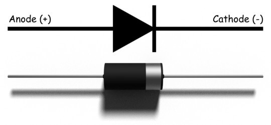
Yes, it is only possible if the impedance plays some tricks. So, the very first conclusion that can be drawn for the systems that create electrical pollution is that they don’t have constant impedance in one time-period of voltage cycle applied across it, hence they draw non-sinusoidal currents from source. These systems are called non-linearloads or elements. Like this most popular guy:
The diode
Note that the inductive and capacitive impedances are frequency variant and remains fixed over a voltage cycle for fixed frequency that’s why resistors, inductor and capacitor are linear loads. In this modern era of 21st century the power system is cursed to be literally littered with these non-linear loads and it is estimated that in next 10-15 years 60% of total load will be non-linear type, well the aftermath of COVID19 has not been considered.
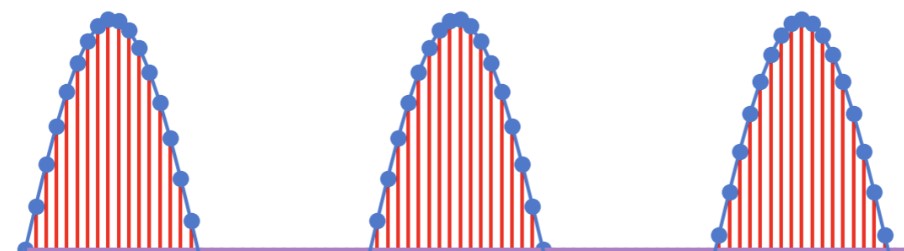
The list of non-linear loads includes almost all the loads you see around you, the gadgets- computers, TVs, music system, LEDs, the battery charging systems, ACs, refrigerators, fluorescent tubes, arc furnaces, etc. Look at the following waveforms of current drawn by some common devices:
Typical inverter Air-Conditioner current waveform (235.14 V, 1.871 A)
Source: Research Gate
Typical Fluorescent lamp
Source: Internet
Typical 10W LED bulb
Source: Research Gate
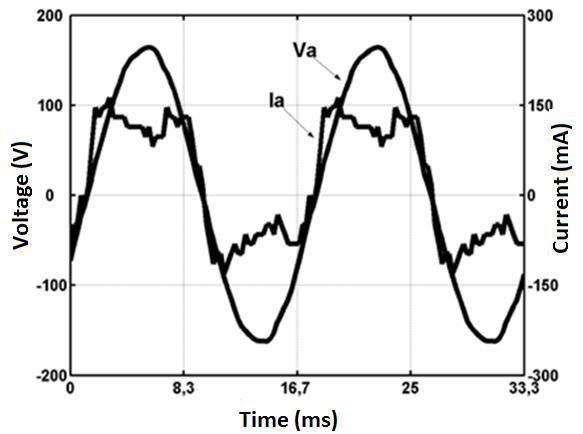
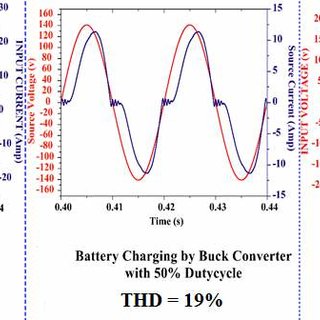
Typical battery charging system
Source: Research Gate
Typical Refrigerator
Source: Research Gate
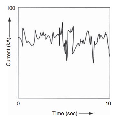
Typical Arc furnace current waveform
Source: Internet
Name any modern device (microwave-oven, washing machine, BLDC fans, etc.) and their current waveforms are severely offbeat from desired sine-type, given the no of such devices the electrical pollution becomes a grave issue for any power system. Now the pollution in electrical power system is not a phenomenon of this 21st century rather electrical engineers have struggled to check the non-sinusoidal waveforms throughout 20th century and one can find description of this phenomenon as early as in 1916 in Steinmetz ground-breaking research paper named “Study of Harmonics in three-phase Power System”. However, the source and reasons of power pollution have ever-changing since then. In early days transformers were major polluting devices now 21st gadgets have taken up that role, but the consequences have remained disastrous.
WAIT, WAIT, WAIT…. What’s that “Harmonics”?
Before we even introduce the harmonics let just apply our mathematical rigor in analyzing the typical non-sinusoidal waveforms, we encounter in the power system.
THE NON-SINOSOIDS
From the blog on Fourier series, we were confronted with one of most fundamental laws of nature:
Any continuous, well-defined periodic function f(x) whose period is (a, a+2c) can be expressed as sum of sine and cos and constant components. We call this great universal truth as the Fourier Expansion, mathematically:
Where,
Square-wave, the output of the inverter circuits:
For all even n:
For all odd n:
Just for some minutes hold in mind the result’s outline:
We will draw some very striking conclusions.
Now consider a triangular wave:
The function can be described as:
Calculating Fourier coefficients:
Which again simplifies to zero.
So, we have-
Applying the integration for each interval and putting the limits:
For even n,
=0
For odd n,
=0
😂😂😂
Now,
For even n:
=0
😂😂😂
Are these equations kidding us???
For odd n:
So finally, summary of result for the triangle waveform case is as follows:
Did you noticed that if these two waveforms were traced in negative side of the time axis than they could be produced by:
This property of the waveforms is called the odd symmetry. Since sine wave have this same fundamental property hence only components of sine waves are found in the expansion.
Now consider this waveform:
This waveform unlike the previous two cases, if the negative side of waveform had to obtained than it must be:
Now this is identified as the even symmetry of waveform, so which components do you expect sine or cos???
The function can be described as:
Here again,
For the cos components:
This equation reduces to:
For the sine components:
This equation reduces to Zero for all even and odd “n”.
Well we have guessed it already🤠🤠.
Summary of coefficients for a triangle waveform, which follows even symmetry is as follows:
Very useful conclusions:
a0 = 0: for all the waveform which inscribe equal area with x-axis, under negative and positive cycle. This happens because the constant component is simply the algebraic sum of these two areas.
an = 0: for all the waveform which follows odd symmetry. Cos is an even symmetric functions, it simply can’t be component of a function which is odd symmetric.
bn = 0: for all the waveform which follows even symmetry. by the same logic sine function which is itself odd symmetric, cannot be component of an even symmetry.
The fourth very critical conclusion which can be drawn for the waveforms which follow this is:
Where T is time period of waveform.
For then the even ordered harmonics aren’t present, only odd orders. This is property is identified as half-wave symmetry, and are present in most power system signals.
Now, these conclusions are applicable to the numerous current waveforms in the power system. Most of the devices with which we have begun with were seemed to follow the above properties, they all are half-symmetric and either odd or even. These conclusions result in great simplification while formulating the Fourier series for power systems waveforms.
So, consider a typical firing angle Current:
So, apply the conclusions drawn for this case. Since the waveform has no half-wave symmetry but is odd symmetric.
The Harmonics
Hope you had enjoyed utilizing the greatest mathematical tool and amazed to break the intricate waveforms into fundamental sines or cosines.
“Like matter is made up of fundamental units called atoms, any periodic waveform consists of fundamental sine and cosine components.”
It is these components of any waveform, which we call in electrical engineering language the Harmonics.
The Mathematics gives you cheat codes to understand and analyze the harmonics. It just simply opens up the whole picture to very minute details.
So, what we are going to do now, after calculating the components, the harmonics?
So first all we need to quantify how much harmonic content is present in the waveform. The term coined for this purpose is called total harmonic distortion:
THD, total harmonic distortion:
It is a self-explanatory ratio, the ratio of rms of all harmonics to the rms value of fundamental.
Now since harmonics are sine or cos waves only so the RMS is simply:
same definition the RMS of fundamental becomes:
So, THD is:
The next thing we are concerned about is power. So, we need to find the impact of harmonics on power transferred.
Power and the Power Factor
The power and power factor are so intimately related. It becomes impossible to talk about power and not of power factor.
So, the conventional power factor definition for any load (linear and non-linear load) is defined as the ratio of active power to the apparent power. It basically is an indicator of how well the load is able to utilize the current it draws; this statement is consistent with statement that a high pf load draws less current for same real power developed.
Where
Active power is: average of instantaneous power over a cycle
Assuming the sinusoidal current and the voltage have a phase difference of theta, the integration simplifies to:
2. Apparent power is by its name simply VI product, since quantities are AC so RMS values.
The pf becomes cos(theta), only when waveforms are sinusoidal.
NOTE: The assumption must be kept in mind.
So, what happens when the waveforms are contaminated by harmonics:
There are many theories for defining power when harmonics are considered. Advanced once are very accurate and older once are approximate but are equally insightful.
Let the RMS of the fundamental, first second, the nth component of voltage and current waveform be
The most accepted theory defines instantaneous power as:
Expanding and integrating over a cycle will cancel all the terms of sin and cos product, and would reduce to:
Apparent power remains the same mathematically:
Including the definition of THDs for voltage and current the equation modifies to:
Now this theory uses some important assumptions to simplify the results, which are quite reasonable for particular cases.
Harmonics contribute negligibly small in active power, so neglecting the higher terms:
2. For most of devices the terminal voltages don’t suffer very high distortions, even though the current may be severely distorted. More on this in next section but for now:
So,
WHAT’S THE CONCLUSION?
The power factor for a non-linear load depends upon two factors, one is cosø and the another is current distortion factor.
If we wish to draw less current, we need to have high overall power factor. Once cosø component is maximized to one, then distorted current sets the upper limit for the true power factor. Following data accessed by virtue of sciencedirect.com will make it visualize better how much significant the current distortion are.
Notice the awful THD for these devices, clearly, it severely reduces the overall pf.
However, these dinky-pinky household electronics devices are of low power rating so current drawn is not so significant, if they were high powered it would have been a disaster for us.
NOTE: For most of the devices listed above the assumption are solidly valid.
Are you thinking of adding a shunt capacitor across the laptop or the electronic gadgets to improve power factor to get low electric bills, for god sake don’t ever try, your capacitor will be blown in air, later we will understand!!!
These harmonics by a phenomenon of “Harmonic Resonance” with the system and the capacitor banks, amplify horribly. There have been numerous industrial catastrophes that have occurred and still continue to happen because people ignore the Harmonic Resonance.
Our Prof Rakesh Maurya had been involved in solving out one such capacitor bank burn-out issue with Adjustable Speed Drive (ASD) at LnT.
Harmonics Generation: Typical Sources of harmonics
Most of the time in electrical engineering transformers and motors are not visualized as:
Instead, it is preferred to see transformers and electrical motors like this, respectively:
These diagrams are called the equivalent circuits, these models are simply the abstraction developed to let as calculate power flow without considering many unnecessary minute details.
The souls of these models are based on some assumptions which lead us to ignore those minute details, simplify our lives and give results with acceptable error.
Try to recall those assumptions we learned in our classrooms.
The reasons for harmonics generation by these beasts lie in those minute details.
Transformers
It is only under the assumption of “no saturation” that for a sinusoidal voltage implied across primary gives us sinusoidal voltage at secondary.
Sinusoidal Pri. Voltage >>> Sinusoidal Current >>> Sinusoidal Flux >>> Sinusoidal Induced Sec. EMF
With the advancement in material science now special core materials are available which saturates rarely, but the older and conventional saturated many times and are observed to generated 3rd harmonics majorly.
Details right now are beyond our team’s mental capacity to comprehend.
Electrical Motors
From this stand-point of cute equivalent circuit the electrical motors seem so innocent, simple RL load certainly not capable to introduce any harmonics. But as stated this abstraction is a mere approximation to obtain performance characteristics as fast and reliably as possible.
Remember while deriving the air-gap flux density it was assumed that the spatial distribution of MMF due to balanced winding is sinusoidal, but more accurately it was trapezoidal, only fundamental was considered. Due to this and many other imperfections, motor is observed to produce 5th harmonics, largely.
NOTE: Third harmonics and its multiples are completely absent in three-phase IMs. Refer notes.
Semiconductors
Disgusting, they don’t need any explanation. 😏😏😏
Effects
Power Loss
Most common, however least impactful effect of power harmonics are increased power loss leading to heating and decreased efficiency of the non-linear (devices that causes) and also later we will learn it affects linear devices too, that are connected to the synchronous grid.
The Skin Effect:
Lenz law states that a conducting loop/coil always oppose the change in magnetic flux linked by it, by inducing an emf which leads to a current.
Consider a rectangular two-wire system representing a transmission line having here a circular cross-section wire carrying a DC current I.
Now one loop is quite obviously visible, the big rectangular one. The opposition to change in magnetic field linked by this loop gives us transmission line inductance.
NOTE: THE INDUCTANCE AND LOOPS OF CURRENT ARE FACET OF SAME COIN, ONE LEADS TO ANOTHER. Think about it!!!!
At frequencies relatively higher than power frequency 50 Hz, another kind of current loops begin to magnify. So, as we said this will cause another type of inductance.
Look closely the magnetic field inside the conducting wire is also changing, as a result, inside the conductor itself loops of currents called eddy current set up, which lead to some dramatic impact.
EDDY CURRENT ARE SIMPLY MANIFESTATION OF SIMPLE LENZ LAW, RESPONSE OF A CONDUCTING MATERIAL TO CHANGING MAGNETIC FIELD.
Consider two cases, a current element dx at r and R distance from the center. Which current element will face greater opposition by the eddy currents due their changing nature??
Yes, true, the element lying closer from the center, as the loop area available is more for eddy currents, this difference in opposition from the eddy current to different elements cause the current distribution inside the conductor to shift towards the surface as least eddy current opposition would be there.
A technical account for this skin effect in given in this manner:
The flux linked by the current flowing at the center region is more than the elements of current at outer region of cross-section;
Larger flux linkage leads to increased reactance of central area than the periphery;
Hence current chose the path of least impedance, that is surface region.
Eddy current phenomenon is quite prevalent in AC systems. Since the AC systems are bound to have changing magnetic fields thus eddy currents are induced everywhere from conductors to transformer’s core to the motor’s stator, etc.
Now when higher frequency components of harmonics are present in the current, the skin effect becomes quite magnified, most of the current takes up the surface path as if central region is not available which is equivalent to reduced cross-section i.e. increased resistance, hence magnified joule’s heating (isqR). Thus, heating is increased considerably due these layers on layer reasons (one leads to another).
Other grave effects include false tripping, unexplained failures due to the mysterious harmonic resonance.
All of these motivated us to build our own harmonic analyzer, follow up the next blog.
The Building Code is an instrument providing guidelines for regulating the building construction activities across the country. Building codes are generally intended to be applied by architects, engineers, interior designers, constructors, and regulators but are also used for various purposes by safety inspectors, real estate developers, and others. Codes that regulate the design and construction of structures were adopted into law.
Why Building Code?
A building code (also building control or building regulations) is a set of rules that specify the standards for constructed objects such as buildings and non-building structures. Buildings must conform to the code to obtain planning permission, usually from a local council. The primary purpose of building codes is to protect public health, safety, and general welfare as they relate to the construction and occupancy of buildings and structures. The building code becomes the law of a particular jurisdiction when formally enacted by the appropriate governmental or private authority.
History of Building Code
King Hammurabi enacted the first known written building code in Babylon in 1758 B.C. written in stone. The code doesn’t have a guideline on how to work and what steps to use. Instead, it states that “If a builder has built a house for a man and his work is not strong, and if the house he has built falls in and kills the householder, that builder shall be slain.”
After the great fires in London in 1666 and Chicago in 1871, building codes started addressing the risks one building posed to adjacent buildings and the public. Denser development in cities, and hazards associated with proximity and taller buildings, led to regulations for the construction of common walls between buildings and outlawing dangerous practices like wooden chimneys. Problems in existing buildings led to codes for light and ventilation, fire escapes, toilets and sanitary drains, and stairs and railings.
In 1905, the US organization, the National Board of Fire, created the first National Code to minimize risk. By 1940, the United States had three regional code organizations, each with its own code. These three organizations and their codes were consolidated into the International Code Council (ICC), and the first set of “I-codes” was published in 2000. These codes include the International Building Code (IBC), the International Residential Code (IRC), the International Energy Conservation Code (IECC), as well as mechanical, plumbing, fire and other codes.
Types & Classification of the current building structure
There are instances when some local jurisdictions choose to develop their own building codes. A long time ago, all major cities in the United States had their own building codes. However, due to the ever-increasing complexity and cost of developing building regulations, virtually all municipalities in the country have chosen to adopt model codes instead. For example, in 2008, New York City abandoned its proprietary 1968 New York City Building Code in favor of a customized version of the International Building Code. The City of Chicago remains the only municipality in America that continues to use a building code the city developed on its own as part of the Municipal Code of Chicago.
In Europe, the Eurocode is a pan-European building code that has superseded the older national building codes. Each country now has National Annexes to localise the contents of the Eurocode.
Similarly, in India, each municipality and urban development authority has its own building code, which is mandatory for all construction within their jurisdiction. All these local building codes are variants of a National Building Code, which serves as model codes providing guidelines for regulating building construction activity.
Classification
Under the building code, constructed building or newly built structures can be classified on the following basis-
Use and Occupancy
Types of Construction
Use and Occupancy
The IBC has ten main occupancy groups as well as multiple subgroups. The occupancy group or subgroup defines the specific use of the building. Subgroups are numbered based on the perceived risk for the building occupants. The lower the subgroup number, the higher the perceived threat.
In many cases, a building has space that may be classified under more than one occupancy group. These multi-use buildings are identified as a Mixed occupancy type. However, if a building space can be considered as either an Accessory occupancy or an Incidental Use area, it may become part of the leading occupancy group.
Occupancy type determines the vertical live loading requirements for the building structure. For higher-risk buildings such as a fire station, school, or theatre, lateral loads (e.g. wind and seismic) and snow will require increases to the loading requirements.
OCCUPANCY GROUP
SUBGROUPS
USES INCLUDE
Assembly
Groups A-1, A-2, A-3, A-4, & A-5
Gatherings – civic/religious/social/recreational
Business
Group B
Office/Professional or Service Transactions
Educational
Group E
K-12 Schools (some Daycare)
Factory/Industrial
Groups F-1 & F-2
Manufacturing/Fabrication/Packaging
High Hazard
Groups H-1, H-2, H-3, H-4, & H-5
Hazardous Materials
Institutional
Groups I-1, I-2, I-3, & I-4
Assisted Living/Hospitals/Prisons
Mercantile
Group M
Display & Sale of Merchandise
Residential
Groups R-1, R-2, R-3, & R-4
Housing/Apartments/Hotels
Storage
Groups S-1 & S-2
Non or Low-Hazardous Storage (including parking garages)
Utility & Miscellaneous
Group U
Accessory Structures
Construction Type
Construction Type identifies the type of materials utilised for constructing a building and classifies the level of combustibility and fire resistance associated with the building elements of a structure. These building elements are required to have a fire-resistance rating of 0, 1, 2, or 3 hours, which indicates the amount of time it can continue to confine a fire and also maintain a level of structural integrity.
Table 601 of the IBC* identifies the fire-resistance requirements of building elements for the five construction types:
Types I and II – All building elements are of non-combustible materials.
Type III – Exterior walls are of non-combustible materials or fire-retardant wood framing with a 2-hour fire rating or less and interior building elements are of any code permitted materials, combustible or non-combustible.
Type IV – Heavy Timber (HT) construction. Exterior walls are of non-combustible materials or fire-retardant wood framing with a 2-hour fire rating or less, and interior building elements are of unconcealed solid or laminated wood members that meet minimum dimension requirements required by the code.
Type V – Structural elements, exterior walls, and interior walls are of any materials permitted by the code, combustible, or non-combustible.
For construction types I, II, III, and V, structural building elements must also be classified as either A or B, resulting in a total nine kinds (i.e. Types IA, IB. IIA, etc.):
A = Protected – Structural members have additional fire rating coating or cover using spray-on, sheetrock, or other approved method that increases the fire-resistance rating by at least 1-hour.
B = Unprotected – Structural members have no additional coating or cover.
Above is a team of thousands of different power modules, better known as the control room of a power plant.🦾
Are you ready to know one of them???
INTRODUCTION
Control and measurement of system parameters is a crucial facet for reliable and safe operation of any electrical systems, particularly for real-time system. By real-time system we mean the system whose parameters like current, voltage, impedance, power, etc. changes with time, thus to maintain the parameters under threshold limits, we first require to monitor them i.e. take measurements in real-time.
For most of the electrical circuits, the voltages and currents are two parameters of greatest interest, as they are solely responsible for safe operation. When unchecked one leads to electrical breakdown and another a thermal breakdown.
Consider the following cases:
A battery backup system, constant monitoring of battery terminal voltage is necessary to stop the battery from getting over-discharged. Also, current drawn has to be monitored to check that the battery doesn’t overheats and catch flames.
In the power system, bus voltages and currents in line have to be maintained very precisely, which again requires first taking measurements.
For metering of electrical energy consumed by a consumer, we need voltage, current and power factor measurement.
Majority of control systems in industrial system employ a negative feedback technique which essentially requires sampling/monitoring of a particular output parameter, which is itself a form of measurement.
PREREQUISITES
KVL and KCL, 😅😅 rest leave on us!!!
THE PROJECT IN SHORT:
Under this project, we set out to build a dynamic power module for measurement of current and voltage in DC circuits and current, voltage, power factor and frequency in AC systems in real-time to constantly monitor them and trigger necessary safeguards.
It’s pretty obvious that real-time operations are best executed with the help of microcontrollers. Microcontrollers are equipped with a group of pins called ADCs which basically read analog voltage level and convert them to n-bit digital data. Problem is that these microcontrollers can hardly survive above 5 V pressure.
So, if we wish to measure higher AC/DC values then we are required to take proper samples of voltage and current, then do proper conditioning, and finally process the data to compute the parameters.
ARDUINO UNO and ADC
With first boards appearing in 2005, Italy based Arduino.cc is open-source software and hardware company which gives a range of affordable microcontroller. With a broad computational power range, they are easy to use platform for purposeful use in industry, education, art etc.
Atmel based Arduino UNO introduced in year 2010 with 32KB of flash memory is best suited to serve the purpose for this module.
Now we are interested in ADC function, for that Arduino UNO has following specifications:
The meaning of these specifications is:
“UNO contains 6, 10-bit channels for analog to digital conversion. It maps analog input voltage at these pins from 0-5 V into integer values between 0- 1023, yielding a resolution of 5V/1024 or 4.8828 mV/unit. It takes 100 usec to read one input, so max reading speed is 10000 times a second.”
Syntax assigned is analogRead(pinname). It reads pin “pinname” and returns 10-bit int accordingly.
A basic voltage divider with appropriate resistor values can be used to scale down higher voltages V to microcontroller compatible levels, Vs.
Suppose readings are to be made in 0-50 V range. We need to scale down this 0-50 V range to 0-5 V.
Now current has to maintained as minimum as possible, to reduce errors. Let current be 0.5 mA. R1 should be of 100K range (5/0.5m). So,
As already stated, UNO has 10-bit resolution so voltage from 0 to 5V would be mapped into integers value from 0 to 1023, which is 5/1023 =4.88 mV per unit, which is fairly good accuracy.
The digital data from ADC can be easily used to manipulated to get the actual voltage, as follows:
GETTING LARGER RANGE
For a range of 500 V:
For current to be 0.5 mA, R1 should be of 1M range (500/0.5m). Thus,
Which is not a standard value so let R2 be 10K.
New scale is:
Putting the value of Vs:
DC CIRCUITS MEASUREMENTS
What we just did was for DC voltage measurement in 0-500V range.
AC CIRCUITS MEASUREMENTS
For AC measurement we have to make few modifications. As voltage range is only +ve (0 -5 V) so we need to either shift whole waveform above zero, or flip the negative cycle or simply chop it, and then take readings. Using suitable algorithms, AC values (RMS/ PEAK) could be found.
READING RMS: Since UNO takes 100 usec for every reading. For a typical frequency of 50 Hz, a half-cycle consisting of 10 msec, so UNO can make 10m/100u or 100 readings. For these 100 readings, the formula to compute RMS can be applied as follows.
Sampling a half-sino, Image courtesy: Internet
READING PEAK:
Using sampling: Max value from the 100 readings from can be found out using some sorting algorithm and RMS can be simply computed from it.
Using time-delay: Since peak occurs at t/4, so using a timer function to generate a time delay of 5 msec after zero crossing and then taking the reading would directly give the peak value.
Any of these three techniques can be used for AC measurement.
IMP: It might possibly be case that the waveform may not be crossing the zero when the ADC starts taking measurement case would result in wrong results or the ADC never captures the maxima case 2a will be faulty , to deal with this is to take a larger number of samples like 2000-3000 to reduce the probability of error occurring.
Sample code for case2a:
The above code can also be used to measure DC voltages.
The final circuit becomes:
Since the sample voltage can be directly fed to microcontroller so no conditioning is required. Let’s see is that the case for current measurement too???
CURRENT MEASUREMENTS
The underlying idea to measure current is to obtain proportional voltage samples for any given load current, read voltage value at ADC port and process the ADC output bit to get the current value.
A proportional voltage can be obtained simply by forcing the current through pure resistor. If the value of this resistor is extremely small compared to the load resistance the equivalent load impedance would hardly change thus load current remain the same and in turn a small but proportional voltage drop is obtained across the external resistance.
Assuming the load current range from 0-2 A. Keeping the external series resistance R, as small as 0.1Ω, the sample voltages will be in range of 0- 0.2 V i.e. (0 -200 mV).
Accuracy would be significantly compromised for small load current if this range of sample voltage is used at ADC.
GETTING LARGER RANGE
Here the sampled voltage requires a proper conditioning.
So, all we need to do is to boost up the sample voltage from 0-200 mV to 0-5 V range.
How would you do that???
Well this is a typical day-job in analog engineering. Technically this is called the signal amplification. Giving a signal a required gain to push the level to a higher value.
The Operational Amplifier
Let us just step back from the current project and take a dive to depths which is certainly not required as far as the project is concerned, but for the sake of spirit of learning more and better, in the name of love of subject. 🍹🍹
What are the Operational Amplifiers?
This class of devices singly forms the backbone of the modern analog industry. Just as the gates in digital electronics, the induction motor in power systems, the IC engine in mechanical systems, the library functions in the computer engineering field, these operational amplifiers are the basal workhorses of the modern analog systems. These little beasts are characterized by a versatile application, which includes amplifier, voltage source, current source, filters, actuator driver, comparator, etc.
The very first need for amplifier circuits typically appeared in long telephone lines to obtain proper signal conditioning at the receiving ends. The problem of the available amplifier in those days were their highly undependable gain due to the inherent nature of the active components used, vacuum tubes in 1930s and transistors after 1947. The gain varied enormously for small changes in working temperature and supply voltage. External condition like season, weather, humidity all of them made the gain of amplifier almost uncontrollable.
Harold Black, an electrical engineer at the bell laboratories in 1927 came up with a revolutionary technique that has now became so ubiquitous in all electronic circuit for control applications, it is called the negative feedback concept.
THE BIG IDEA: Use an amplifier made of undependable active elements to get a very large gain, typically infinite, and then use dependable passive element to provide negative feedback to it to obtain any reduced desired gain or transfer function.
This remarkable concept is the underlining principle of all the practical operational amplifiers used today.
Now to understand op-amp, as known popularly, there are two standpoints. One is this:
Image courtesy: Internet
And the other is this:
And we have no doubt that you would like to understand it through the second stand point.
Now recall the first part of the basic idea i.e. building infinite gain op-amp, more or less this comes under the domain of pure analog electronics but given the versatility of operational amplifier the second part of basic idea, the design of negative feedback circuit using passive elements (resistors, capacitors, inductors) comes under the realm of the electrical engineering. Also, it largely deals with core electrical circuit theories like KVL, KCL, Thevenin’s, etc.
The first standpoint leads to accomplishment of first part of the basic idea, and the second stand-point leads to the realization of second part of the idea.
Now you would wonder how can we execute second part without knowing the first part, and here comes a great powerful tool to do this for you, it is the hack of all the complicated system around us.
“THE ABSTRACTIONS”
Without a solid-thorough understanding of how that horrendously intricate mesh of transistor and resistances work to produce infinite gain, we can still build a perfect negative feedback circuit to obtain exact desired transfer function (gain), using the abstractions.
This concept is so crucial and pervasive in building all modern perplexing systems the microcontrollers, computers, airplanes, particle accelerators, etc.
Consider this more striking example: the “printf” library function which we take for so granted, is an abstraction of the all the icky logics that goes into it to print a given string on some terminal or a display device. Try building your own function to print a string, you would be shocked at the complexity behind this little command.
The point is that we cannot keep on dwelling on basal stuffs if we wish to build something magnificent, if we do-we will never end up building an app, a website, a power converter, and so forth.
So, use of abstraction is a proven tool to reduce complexity, we can use this tool to derive some common results and build or understand large systems layer by layer.
What you see below is the abstraction of the mesh of transistor shown earlier.
WHAT DOES OP-AMP DO FOR US?
Well, they just simply produce output proportional to the difference in the voltage between the two input terminals. The proportionality constant is very high, order of 10^5, called the system gain, note Ed is in μV and o/p in V.
Mathematically,
The output characteristics for the device is as follows:
The magnitude of output voltage depends on the difference between in the input terminal voltage in active region and it saturates once output hits the supply voltage magnitude.
The polarity of output is same as the polarity of V+ wrt V-, thus V+ is called non-inverting terminal.
THE REAL OP-AMP
The variety of op-amps available are many LM324, LM339, LM258, etc. Most popular is IC 741. In our project we will use LM358, as it is single supply dual op-amp, so it will reduce complexity a bit.
Image courtesy: ON Semiconductors
THE RULES OF OPERATION
The difference in input voltage is very small (typically in μV) so the two input terminals can be assumed to be virtually shorted, i.e. at same voltage.
The input impedance is very high, so both the input currents are zero.
The gain is infinity.
This is all one need to know about op-amp, using these three rules op-amps can be used very easily to get required gain.
Let’s check it out.
ROUTINE EXAMPLES
Inverting configuration:
Just calmly apply the rules one by one.
Input terminals at same voltage, so voltage at 2 is voltage at 1, i.e. zero.
No current through input terminals. Apply KCL at terminal 2:
The characteristics become:
Non-inverting configuration:
Again, apply the same rules:
Input terminals at same voltage, so voltage at 2 is voltage at 1, i.e. V1.
No current through input terminals. Apply KCL at terminal 2:
The output characteristics become:
So, are you now able to appreciate the beauty of these curves we just obtained??? We began with an op amp with typically infinite gain (10^5), showing very creepy dependence on the temperature and external factors and here is a calm stable op-amp with desired finite gain by just using simple passive resistances.
New gain of system become (Rf/Rb) and (1+ Rf/Rb), which remains fairly constant for a wide temp range.
HOW THE NEGATIVE FEEDBACK WORKS?
Though equations obtained by reasonable mathematical approximations shows us independence of overall gain, but intuition is still lacking….
So, how does the results we just obtained is manifested actually????
So, lets simply heat an op-amp working in a non-inverting configuration, and see what happens.
As heating begins the gain begins to rise, and so does the output voltage. Corresponding to it there will be rise in voltage at terminal 2. Which would result in lowering the difference between the two input terminals, and consequently the output drops. This drop in output leads to drop in voltage at terminal 2 which results in increased differential voltage resulting in increased output. These oscillations die out soon and result is stable output displaying temperature independent gain. This is in general how a negative feedback principle works.
IMPORTANT
Ensure that the power is never off when the inputs and output are connected in the op-amp.
……………………………………….
So, it’s time to get back from where we left, the need to boost up the sample voltage from 0-200 mV to 0-5 V range.
Pretty cakewalk now, isn’t???
You would say it’s a lockdown. Where should I get the op-amp?
Cool, there are whole lot of gadgets and sensors where you can find it.
Say, for example, we extracted an op-amp from an IR sensor.
Due to unavailability of any solder iron, we just simply cut out the resistors, IR LEDs, POTs.
Using careful examination of the IC we traced out the whole IC circuit diagram.
And simply bought out the required terminals of op-amp by normal connectors.
To boost the sample voltage from 0-200 mV to 0-5 V range, we need a gain of (5/200m = 25), since inverting is not desired hence using the non-inverting configuration.
where,
Required gain is 25.
Let the resistances be:
Finally, we used pair of resistors in combination to get the required ohms and made the op-amp circuit with a gain of 24.6 as follows:
DC CIRCUITS MEASUREMENTS
What we finally got is a 0-5 V scale that would end up giving us 0-1023 integer, we have to get all the way back to current, lets gooooo!!!!!🚀🚀🚀🚀🚀
Analog Voltage at the ADC:
Voltage input to the non-inverting amplifier:
Current through the external resistance:
The overall conversion factor becomes:
Putting our design values:
AC CIRCUITS MEASUREMENTS
Contribute
FREQUENCY AND POWER FACTOR MEASUREMENT
Underdev
DISPLAY LCD
All about LCD interfacing with the Arduino can be very easily understood by referring this short 1 min read at Arduino.cc.
We tried the same, followed every step very accurately but unfortunately, results didn’t show up except this blank screen.
Help us to troubleshoot the problem by coming up with possible errors.
We build the icky circuit thrice from zero, and then checked and rechecked every connection, but failed.
MORAL:
Life isn’t fair always, sometimes no matter how hard we try, no matter how dedicated our purpose is, we are destined to fail. We have realised this truth, and we hope to develop temperament to mindfully accept such failures in life.
Connecting the circuit three times hadn’t yielded us the result, but surely planted in us the seed of perseverance to go through that nasty process. Surely, we raised our patience wall a little higher.
And it is these lessons and quality we wish to learn and develop by involving in these projects, not just simply putting things up.
THE FINAL CIRCUIT
Well do you think it’s done???
No, it’s not.
Since we are using same apparatus for the measurement of AC and DC. We hadn’t done anything to identify them. It can be done via program codes or by hardware.
By providing high or low manually on a digital pin we can indicate the microcontroller about it, say high for AC measurements and low for DC measurements.
We could arrange a low resistance of required power handling capacity, so current measurements cannot be made. Moreover, the resistors required for the voltage multiplier are also not available with us. So, we used op-amp to get the required gain, slight code modifications and obtained the results using the serial monitor. Battery voltage is 12.25 V power module shows 12.33 V, 0.65% error.
CONCLUSION
These power modules can be custom build for battery monitoring for systems like drones, etc. by removing AC measuring components and using small uC like Arduino NANO. They could be used for real-time monitoring of some load. They could be used to trigger some protective measures like triggering a relay, blowing a buzzer, etc. when any parameter beyond a limit.
The development or building of measurement systems is less about dwelling on rigorous electrical concepts rather more appropriately it could be categorized as a form of art, which requires small intuition of some very basic electrical phenomenon and rest is all about creativity to obtain the desired result by arranging the already available elementary elements.
If we could imagine force exerted on a wire carrying current in a magnetic field, if we can imagine emf induced in a changing magnetic field, if we can imagine magnetic field due to a coil carrying current, we are ready to go, about learning, understanding, modifying and building interesting measurement systems.
🍹🍹🍹
Keep reading, keep learning
AANTARAK DIVISION,
TEAM CEV!
References
Special thanks to Prof Varsha Shah
MIT OCW 6.002 Circuits and Electronics
Mr Anand Aggarwal’s Fundamental of Analog and Digital Electronics
In the previous blog “Inverter Circuits: The Basics”, we have begun with the very raw idea of DC to AC conversion and methodically we developed our basic circuit for obtaining a typical square waveform having power frequency from a constant voltage DC source.
We have understood the working of the circuit. Now for the purpose of practical implementation, all we require is the triggering circuit for the two MOSFETS at required frequency, proper dimensioning of the elements to check the reliable and safe operation, and also a filtering circuits to couple the load with our inverter circuit.
Let us introduce an exciting new class of electronic instrument…
Multivibrators
Multivibrators forms a wide class of electronic circuits and deals with two states (namely high and low) in different possible ways. Generalized diagram of a multivibrator:
They are a total of three kinds:
Monostable Multivibrators: this sub-class is stable only in one of states, say high (1). So, once triggered by some external signal then the circuit enters into its unstable state i.e. low (0) and returns back to its stable state 1 after some pre-fixed time-period. Example of these types of circuits are delay generator, timing circuits, etc.
Bistable Multivibrators: these circuits are stable in both the states (1 & 0), so if multivibrator is in high states and if triggered by some external signal its state changes to 1 and remains 1 until the next trigger. In simple words an external signal just flips the current state of output. Example of these types of circuits is flip-flops.
Astable Multivibrators: they are unstable in both states, thus if you give trigger/supply to them the keep on oscillating between the two states indefinitely. They find extensive use in timers and oscillators.
We are only interested in astable multivibrators, for generating the timing pulse for biasing of the MOSFETS. There is a great range of IC that gives this mode of operation of continuous oscillation on a single trigger, the most popular of all ICs is timer LM555, in 4000 IC series we have CD4047, CD4049, CD4093, etc.
Understanding the Circuit Elements
Understanding the working and principle of a system comes under physics or pure science domain but realizing those systems by considering the real-world parameters and the effects is what engineering is all about. Element dimensioning, suitability, economics and all those things which come into picture when we try to turn a diagram drawn piece of paper into a real system to transform lives, is an engineering task. For example, working of an Induction motor is a physical phenomenon, but to utilize these machines in such large numbers littered beyond the horizon is only made possible by what we call power system engineering. So, there is a line where the physics ends and the engineering begins.
For an electrical system, it is the task of an engineer to take care of the parameter to be maintained under specified limits- voltage level to check dielectric breakdown and current level to check the thermal breakdown. With this background let us start exploring the circuit elements required in for our inverter.
Battery**
Voltage level, ampere-hour rating, max current rating
Electronic Switch MOSFET
The MOSFET we are going to use is the power MOSFET, modified specially to carry larger current, unlike usual low-power electronic circuits.
The device is identified technically as IRF540, n-channel 100V-0.055 Ohm, 22 A, Low-gate charge Power MOSFET, explained later.
PINS:
It is a three-terminal device numbered 1, 2 and 3 as given:
The pins 1, 2, 3 are gate, drain and the source terminals.
Physics in one line:
MOSFET stands for Metal Oxide Semiconductor Field Effect Transistor, it is a voltage-controlled current device. The structure of the device is such that on the application of voltage at gate terminal a channel between the drain and source is formed which doesn’t exist earlier.
Without and with gate voltage:
If you apply voltage at the gate terminal then for some voltage across drain-source the current begins to flow from (2) to (3). The more the gate voltage larger is current at a given drain-source voltage, which saturate at some point. Graphically:
DATASHEET
As earlier stated, after the physics we now have to look at the engineering part. This MOSFET has a limit on all of which can ve referred from the datasheet.
MAX RATINGS:
Did you noticed the things written along the name of device? Here is what all that mean….
From the output and transfer characteristics it can be concluded that we should strictly restrict the gate source voltage between 4 V i.e. Threshold Voltage to 5 V for saturation current less than 22 A.
In the gate circuit let Vgg the supply voltage be 5V, Vgs be 4 V in on-state and Igs as 10 mA thus the value of resistance in the gate circuit for a given gate excitation voltage. (Refer datasheet)
NOTE: Precise calculation for Ig is still not clear. The team thinks that maximum allowable gate charge and the pulse width has to be taken into consideration to calculate the maximum current that should be limited by the gate resistance. If you can contribute, please contact us.
CIRCUIT:
In the circuit during on-state, the forward resistance between the drain-source is given, thus depending on the Vdd and load resistance the current will flow which should be less than 22 A at 25-degree Celsius.
FUN FACT: It is amazing to know that the device MOSFET is no 1 manufactured electronic device in our entire history with 13*10^12 billion units sold by 2018 since 1964. 🤐🤐🤐🤐
Check out which devices have been the top-selling product since their invention.
IMP HANDLING CARE:
Handling of MOSFET is little bit strenuous job, because it is a delicate device. If the gate, source and drain terminal are not shorted then there is possibility of static charge accumulation at the gate terminal hence forming enough electric field to puncture the ultra-thin silicon-dioxide layer, leading to permanent failure of MOSFET.
Ground yourself when handling MOSFET.
Keep the three-terminals shorted until plugged into the circuit.
Voltage should be applied only after all terminal are connected to the electrical circuit.
The next thing is the pulse generator circuit for proper switching of the MOSFET 1 and 2 to obtain square wave of 50 Hz.
CD4047B
Introduced in the multivibrator section, we are going to use CD4047BE CMOS Low-Power Monostable/ Astable Multivibrator for the generation of required gate pulse.
PINS:
Datasheet describes the 14-terminals of CD4047BE with nomenclature and function of device as listed below:
Cleary we are interested in the Astable mode of operation as the gate pulse required is oscillatory with a 20 ms (1/50Hz) time-period.
The Astable Mode:
Again, datasheet according to the internal circuitry gives the terminal connection.
Calculation of value of external resistance and capacitors:
In the table above the time-period of pulse available at the pin 10, 11 is 4.40*RC seconds. This Q (pin 10) would ve the pulse input to the gate terminal of MOSFET M2 so that the positive square waveform appears across load. In the next half time-period Q will e low thus Q var (pin 11) connected to the gate of MOSFET M1 will e high and hence negative waveform appear across the load.
Assuming that we manage to get the sinusoidal output, the Q pulse and the load voltage waveform will look like:
The required frequency for voltage is 50 Hz, time-period of which is 20 ms, which also becomes the time-period of the pulse Q.
Referring the datasheet, the typical values of resistance and capacitance at which the multivibrator CD4047 produces pulses with greater precision, the value we chose are 45 kΩ and 0.1 μF respectively.
Circuit Diagram
Considering the pin connections, the circuit for the gating of the MOSFET using CD4047E can be obtained as given. The output pins 10 and 11 should be given to the gate terminals of any of M1 and M2 device.
CD4047 being operated in Astable mode, R = 45 kΩ, C= 0.1 uF, Vdd = 12V
NOTE: The voltmeter measures RMS value and the waveform is pulsating DC, peak value has to be considered while calculations.
A visual illustration of pulsating waveform for R and C as 330 kΩ and 0.1 μF:
DATASHEET: MAX RATINGS
For different supply voltages the sink current and source current ratings are indicated as follows. The pulse voltage can also be experimentally determined for given supply voltage.
Thus, for obtaining required gate source voltage pulse, required value of resistor can be connected to interface CD4047 to the IRF540.
NOTE: The current limiting resistor calculation has still to be verified by considering the gate pulse requirement of MOSFET.
Three winding transformers
A three winding transformer is five terminals device as opposed to normal 4 terminal where we have two primary terminals and two terminals on the secondary side.
The basic transformation equation for two winding transformers, was:
Where Vsec and N2 are voltage and turns respectively on the secondary side and Vpri and N1 for primary side.
In this case of three winding transformer this same equation is applicable on individual coil on primary as well as both coils combined.
For individual coil:
Here Vpri is voltage across any one of the primary coils. The transformer is rated as 12-0-12/240 V, 5A.
Hence putting the values, calculated value of turn ratio is:
a.) Measured Voltage across one coil for secondary being excited by mains supply
b.)Measured mains voltage on 21-03-2020 @18:30 HRS
So, actual turn ratio is:
For both coils combined:
According to the given ratings, calculated primary voltage is:
Measured voltage across both the primary coil
Using the turns ratio obtained in previous measurement, actual primary voltage is:
Which is verified by the voltmeter readings. So actual turn ratio is 18.18.
Filters
Choke coil
********
Capacitors
Capacitors are among one of oldest device used so widely in electrical circuits. Their characteristics can be utilized in numerous ways. In DC circuits they act as voltage smother by filtering out ripples (rectifiers), in radio technology they are used for tuning, in industries like automobile and aviation- they are utilized as emergency energy storage banks, in power system they are utilized for power factor improvement resulting in power and voltage regulation, and here we will use it in AC circuits to the block DC voltage.
The equation governing the behavior of capacitor in DC/AC circuits can be easily understood using some textbooks, here we will consider some practical application points.
Now the most important parameters of capacitor are its capacitance, its maximum operating voltage ratings and maximum reactive power handling particularly for high-voltage and power applications.
Capacitance value of 1pf ceramic capacitors to 50,000 uf Electrolytic type to 10F supercapacitors, with different operating voltages are commercially available. Depending on the requirement different capacitor technology can be opted. Consider this insightful graph from Wikipedia which helps in determine the capacitor type for a given requirement.
Photo courtesy: Wikipedia
These commercially available capacitors are broadly divided in two categories:
The polarized capacitors: These are polarity dependent and exclusively used for DC applications.
Electrolytic types: gives advantage of small size and stability for relatively larger C (few uf to thousands uf) compared to unpolarized ceramics-type. Application in DC voltage smothering, etc. Also used in AC fan motors, how. Can you answer???👴👴👴 (0.1 uF – Thousands uF)
IMP: The terminal marked negative should always e connected to the negative polarity of source.
2. Supercapacitors: most versatile category. With higher capacitance, they find applications in the field of electronics (to power memory during power cut-off), transportation, renewables, etc. Though the typical capacitance of single unit is higher but it’s working voltage is mere 2-5 V, so numerous cells are connected in series to obtain the required rating.
Photo courtesy Internet
2. The unpolarized capacitors: These capacitors have no polarity specific terminals. Hence used in both AC and DC applications.
a.) Ceramic type: ideal for smaller capacitance and for wider frequency (specially high) spectrum. Oscillator tuning, HF applications. (1 pF – 0.1 uF).
The meaning of 102 is 10*100 pf and 104 is 10*10000 pf. First two digits are the values and last is the multiplier and value come in pF.
Film-type: More popular in high-voltage and high-power applications like snubber circuits, etc.
Photo courtesy Internet
As far as general projects are considered either ceramic or electrolytic is preferred choice according the capacitance required.
Another important class of capacitors is the capacitors system employed in power systems, which goes far beyond off-topic to be discussed here. However, for purpose of mere excitement and spark curiosity in the readers interested in electrical field this particular stuff, here is view of those massive capacitors systems:
General Electric power factor compensation utility for power grids
Notice that the tiny ceramic capacitor and these megs-structures are also defined by same physical equation Q=CV and all others, and see how engineering has made them strikingly different. A physicist can only give us those equation but it’s the job of engineers to pump life in those dead equations to build some stunning things.
The last circuit:
The actual test circuit working at 50 Hz:
Visuals of circuit operating with 330 kΩ resistance in CD4047:
The Inverter Family😇😇😇:
Conclusion
Making the circuit work as expected was not the final aim of the project which we failed also as of now because of shortage of resources due to corona virus outbreak (low rating battery, choke coil, etc), thus not able to test our circuit on actual AC load.
But the core objective and higher purpose of the initiative which was to develop the critical thinking to build a concept of circuit to obtain desired results for a given set of initial conditions, honing skill to be able to select appropriated element from numerous choices available by considering the suitability, economics, etc., working out the circuit parameters by referring the standard datasheets and be able to work in team was surely achieved to satisfactory level.
References
Drive link to datasheets, important lectures videos and notes, etc:
Meanwhile the documentation of project was done in respect of the man Richard Feynman on whose vision CEV hang so tight:
Science will do help us win over this corona thing, just as it has helped humanity fight influenza and whatnot, till then hold strong and keep believing.
The Renewable energy is showing a great ramp up in these early decades of 21st century era. The trends and prediction show a promising future for solar, wind, tidal etc. The solar energy harnessed in the form of solar photovoltaics and heat are boosting ever since the early 2000s, and in the year 2019 it shot to gigantic 25% growth rate and increasing.
Note: A better-edited version of this blog is available in original MS Word format, link below:
The problem with renewables is not of power scale but of irregular availability. For example, in a single hour, the amount of power from the sun that strikes the Earth is more than the entire human race consumes in a year, a hurricane every second releases the energy equivalent of 10 atomic bombs but last only a few minutes or hours.
However, it an obvious fact that we couldn’t tap tiny fraction of these mighty energy resources due to present technology constraints, but nothing could be so soothing, to hear of energy availability at such minimal cost to our environment when climate scientist predicts of human race extinction due to fossil-fuel induced climate crisis.
The supply and demand cannot be achieved using renewables without proper engineering. Energy storage provides the only feasible solution to link the two. Storing when excess availability and delivering when demand exceeds generation.
There is massive science community working in the area of energy storage technologies: mega batteries, large pumped hydro storage, thermal storage, chemical storage, etc.
Now the other face of story is that the modern power system is in transitional period, now DC power is again gaining ground on consumer side like the highly efficient BLDC motors, semiconductor applications like large database centers, home appliances, and jillion low power devices operating on DC. But still AC is major form of consumption and unfortunately major storage technologies (most importantly batteries) don’t store AC power directly.
And here comes the topic of the blog: The Inverter Circuits.
Inverter Circuits are systems designed for efficient conversion of DC electricity into AC electricity, and comes in wide range of power ratings from small solar charging LED lighting system to medium house emergency system to massive receiving stations of HVDC transmission lines using different conversion principles.
Under this project, team Aantarak aimed to look upon inverter technologies and tried to develop an insightful understanding of the operational principles of inverter circuits, with a vision to further improve the existing technology.
In this first blog intuitive explanation of inverter principle and mathematical analysis of system performance, typically available topologies, major circuit engineering challenges and scope of improvement are explored.
BASIC IDEA OF DC TO AC CONVERSION
Suppose we have V Volts DC battery source and we want to power an AC load whose input is specified as f Hz.
How would you do that, think for a second.
To get an AC supply from a DC source, all we have to do is to interchange the supply terminal across the load at the required rate. So, for 1/2f seconds we are giving +V, then zero and then -V for next 1/2f seconds.
Well that is a square wave.
If you recall the mathematical treatment of waves shapes in previous blogs, the Fourier series expansion of this wave give the component waveforms.
Let square wave be represented as:
Fourier series expansion of the waveform is:
Graphically plotting (in the time domain) the components of a square wave:
Plotting the components in the frequency domain:
But for now, we can say we have obtained a voltage waveform which has a sinusoidal component of f Hz in it along with its multiples.
We will look at implication of multiple frequency components later.
If we try to realize this physical interchanging of the terminals using some electrical/electronic device then we are half done for building an inverter circuit. 🙌🙌🙌
So, let us now use this concept to layout circuit basic idea using some imaginary god-switch which is capable of doing what we want here exactly.
Assume an electrical circuit that works in following manner:
Between load terminals: LT1 and A & D and between LT2 and C & B we have a single pole double throw switch whose operational characteristics could satisfy following operations as described below.
So, for the first half time-period, load should be supplied by +ve voltage, for that:
A & LT1 and B and LT2 must be shorted.
D & LT1 and C & LT2 must not conduct and should withstand voltage appearing across them.
Then for a very small-time instant voltage should across load must be zero.
For that:
A & LT1 and C and LT2 must be shorted or,
D & LT1 and B and LT2 must be shorted.
For another half time-period, load should be supplied by -ve voltage, for that:
D & LT1 and C and LT2 must be shorted
A & LT1 and B & LT2 must not conduct and should withstand voltage appearing across them.
Now the vague principle of interchanging supply terminals to obtain an AC voltage waveform across a load using a constant voltage battery has become much clearer. Before we go on laying out exact switches required at the load terminals, we have to give a thought on the load current waveform too.
Real-world AC load
When the load is purely resistive- things are simple, the load current will follow the voltage linearly and the direction of current would be from A to B I positive cycle, zero current at t=t/2, and reverse direction in next half cycle.
When you search for switches with such characteristics, then the 21st century Doremon pocket’s hobbyist electronics store (Easy Electronics for SVNITians😅😅😅) will give you a BJT.
With proper base supply, we can obtain the desired characteristics.
But when it comes to real-world, rarely you would find an AC load of unity power factor or we can say purely resistive load in another way.
For non-resistive loads, the current through it and the voltage across the terminals are not linear. For inductive load the current will lag and for capacitive load the current would lead.
Consider a case when the voltage across the load somehow obtained is sinusoidal, which will be obtained in advanced inverter circuits.
The load being inductive, will show the following characteristics.
As indicated in the graph at the onset of every -ve half-cycle due to lagging nature, load current won’t reverse its direction similarly for +ve cycle. The above circuitry would reverse the voltage across terminal but it would not be able to sustain the required load current of opposite polarity. This could be easily achieved if we connect a diode to conduct current in short time period at the starting of +ve or-ve voltage waveform.
So, the new circuit now becomes:
Let us try to analyze the circuit operating over one complete cycle.
+VE VOLTAGE WAVEFORM:
From t = 0 to t = T2, transistors T1 and T4 should be ON and transistors T3 and T4 must be in OFF state.
t = 0 to t = T1: Current is negative so diode D1 and D4 will conduct.
t = T1 to t = T2: Current becomes positive hence transistor T1 and T4 conducts.
–VE VOLTAGE WAVEFORM:
From t = T2 to t = T4, transistor T2 and T3 should be ON and transistors T1 and T2 must be in OFF state.
t = T2 to t = T3: Current is positive so diode D3 and D2 will conduct.
t = T3 to t = T4: Current becomes negative hence transistor T2 and T3 conducts.
In the following table we have required states of transistor (T1, T2, T3 and T4) to obtain the AC waveform across the load and which diodes are conducting and not-conducting current during the particular time-period.
We can replace the transistor and diode combination by another power electronics device, called power MOSFET. The greatest advantage of using this device is its capability for conduction of current in both directions. Additionally, it gives more power handling and reliable operation. The device is known by name of IRF540.
Internal Schematic Diagram:
NOTE: The diode shown in the symbol is parasitic. To know more follow the notes or the datasheet of IRF540.
A generalized statement can be made that all the four switches are capable of conducting current in both directions during ON state.
Now let us have a glance on most important parameters of an IRF540 taken for datasheet:
The drain source breakdown voltage is 100V, while most of AC load operate on 230 V RMS voltage i.e. peak value of 325 V. So, this H- bridge configuration is modified for obtaining relatively higher AC peak voltage for low DC battery voltages. This is done by use of a three winding step-up transformer.
In this circuit when M1 is OFF and M2 is ON, the battery injects current to the primary winding (marked 3+) and the voltage appear across the load is +ve. When M1 is ON and M2 is OFF the battery supply the primary winding (marked 2+) and the voltage induces on secondary is -ve (opposite polarity than the first cycle).
Since the MOSFETs can carry bidirectional current through the source and the drain terminal thus this circuit can ve used to power non-linear loads also.
Gate Triggering Circuit
The MOSFETs M1 and M2 should be turned ON and OFF alternatively for 10 ms each for obtaining an AC output voltage of 50 Hz frequency. Numerous IC can be used to design the triggering circuits like IC4047, IC4049, etc.
CONCLUSION
The output voltage wave obtained using the circuit drawn above is a square wave. The Harmonic content would be little more than required for optimal performance.
Using a minor modification to this circuit we can get a modified sine wave.
It resembles more closely to pure sine wave hence improved harmonic performance. In the next blog will see how the harmonic performance is computed, measured and improved in inverter circuits, some practical circuits, and much more.
NOTE: Other advanced technique used is PWM (Pulse Width Modulation) technique.