We thrive by taking nothing for granted!
CEV had its first practical hands-on with MOSFETS when we tried to implement a primitive inverter circuit. Device used was IRF540. Back then we didn’t find it so fascinating, considering it just one chisel in our tool-box like resistors, capacitors and inductors, battery, diodes, etc. Only did we moved forward in our lives we realized how one single device characteristic if carefully manipulated can help us to build so many useful stuffs.
If we look at statistics, MOSFETs is most widely manufactured electronic device or component in the entire 200 years of human technical endeavour. The number in fact overshadows all of the other devices lined up altogether. Wikipedia says the total number of MOSFETs manufactured since its invention is order of 10^22. This is just a number we don’t have anything much familiar to correlate and help understand how really big it is.
10000000000000000000000!
Systems like an ordinary radio contain in order of thousands of MOSFETS to provide enough gain to EM waves to finally yield audible audio signals, the smartphone on an average contains in order of 10 Million, an i5 intel core processor contains in order of 1.5 Billion of them, the power supplies for electronic gadgets we use though utilize another variety of MOSFETS called power MOSFETS. The circuitry (power and control) used in handheld devices like trimmer, hair-dryers, toasters, washing machines (automatic), efficient motor assemblies, cars, airplanes, satellites, space shuttles, particle accelerators and what not………., all of them essentially have insane amount of no. of MOSFETs operating in one of its particular desired regions of operating characteristics depending on analog, digital or power device category, very silently and calmly doing its job it is supposed to.
MOSFETS single-handedly forms the backbone of entire analog and digital electronics. Yes, you heard it right, both analog and digital. It lies at the heart of almost all the basic components which are used to build higher-order circuits or devices.
Wait, wait, we promised ourselves to not take anything for granted so when we say analog and digital electronics what do we mean exactly?
Essentially analog and digital are two ways of playing with signals (of voltage or current). Playing here might literally mean fun like playing a song over a speaker, displaying a video on LCD, LED or CRT, talking with loved ones over cellular network, enjoying a live broadcast of a soccer match and capital FM or even as simple as using TV IR remote to frustratingly switch over news channels which spread crap at 9 PM oooooooorrrrrrr playing could also mean stakes as high as using an ECG and other biomedical sensors and instruments to save lives, sending and receiving radio signals of a pilot messages to ATCs, or implementing something as necessary as what we call www.
It is hard to think all of these sharing anything common, right, but in all of the cases we are simply manipulating signals all the time in order to just somehow do what we want using the analog ways or digital ways or most of times both.
Well, it may be hard to think what signal manipulating exactly means here, nor we intend to talk about the grudging details but what we want to first appreciate is the profound immensity and necessity of the things which we are going to talk about.
Again, taking nothing for granted, the first question to address is what exactly signal manipulation would be using analog way or the digital way?
- The core requirement of real life the Amplification of signals:
Consider all the different kinds of sensors deployed on field to measure any physical parameter of interest like a temperature sensor in Air conditioners, a metal detector at airports, a stain gauge sensor, an antenna for radio waves detection, a heart-beat or pulse sensor, etc. In all the cases we exploit natural phenomenon to get variation of temperature, strain, EM waves, vibration converted to electrical signals (maybe voltage or current variations). The strength of converted electrical signal is by nature too weak for any purposeful use, like displaying the values of temperature or beats per second on some kind of screen, playing the song received on antenna, etc. The circuits that produce these magical outcomes can’t be driven using signals of such feeble power. We need a man-made device which can significantly boost the signal power.
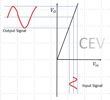
Graphically. Amplification be like:
2. Filtering is another core requirement of real life:
In the electrical signal at the output of any practical sensors, we have by nature something called a noise. These noises are result of different reasons for different systems. To separate the noise from the useful signal based on the characteristics of systems we use signal manipulation technique called filtering, using something called as filters.
3. Along with these basic kinds of manipulation we have another range of signal manipulation, which essentially helps us to do computation. Like mathematical operations like addition, subtraction, integration, etc. can be achieved using voltage dividers, RC circuits, etc.
In these cases, we by default assumed that signal voltage or current can take infinite number of possible levels in between any two finite levels, between 3 V and 4V, our signal can be 3.11V, 3.111V, 3.1111V, etc.
Why go digital, if we can do it all in analog?
Most of time in digital world first we learn how to do it, then do it and only then we understand why we did it. Digital way of doing things is especially advantageous in doing things described in (3).
Digital way is moving from representing infinite levels signals to no levels between signal levels, only two levels called high and low. This doesn’t make direct intuitive sense unless we study them first.
However, some obvious motivating reasons for moving for digital way is inherent noise immunity, and simplicity.
The digital world has its own kind of signal manipulation requirements like inverter (NOT), adding (AND), orring (OR), etc, in general elements which execute these are called gates.
The layer upon layers upon layers…………
All of this begins by looking at nature. Because we are simply restricted to things, she can provide us, no other choice. Our role is to observe, modify and manipulate whatever she can offer us to make some good use for ourselves.
Resistors, capacitor, inductors, battery, semiconductor switches (Diodes and Transistors) all of this forms the most primitive components which are most basic building blocks. Also, in this category we have devices which exploit natural phenomenon like Photoelectric Effect, Piezoelectric effect, etc. to make sensors like photodiode, strain gauge, etc.
Using these components, we build a little higher order systems, say for example a voltage divider (using battery and resistances), a primitive filter circuits (using resistors, caps and inductors), or maybe most importantly the center of this discussion, an amplifier circuit (resistor, transistor, and battery).
The next order of systems now comprises of these little systems as basic blocks. Like an operational amplifier which uses many amplifier circuits and voltage divider bridges. Something called as gates (NOT, NAND and NOR) are also build using the twisting the same basic amplifier configuration and adding more switches, etc. This layer also set forward two categories we lovingly call analog and digital electronics.
The next layer uses op-amps and gates as their building blocks. For examples in analog world, we can have a comparator, a voltage follower, an integrator, a differentiator, an oscillator, etc. And in digital world we can have what we call combinational logic circuits like flip-flops of varieties D, F, JK, etc.
Things getting interesting right, however still not that useful.
The next layers use these elements as building blocks. Using comparators, integrators etc., we can now start making something like trivial voltage, current and frequency measurement units, we can have active filters, a small power supply, and so on. In digital world the notion of time is introduced by using time signal (clock signals), which is a giant leap.
Now we can have these systems deployed for forming part of even bigger layers. In analog domain we can implement control system feedbacks and jillions other circuits called integrated chips (ICs). Digital world however these days go on building more layers of complexities. The layer of assembly languages, and then higher-level languages like C++ all of them takes off right from here. It becomes so far-reaching that entire branch starts up from here, the CS.
Using these same blocks microprocessors are built, computers also somewhere follow up as we go on and on. EEs have limits on how far they can go, so we stop here, to give the lead for Comps folks.
Personal computers and smartphones are most popular example of highly complex layer upon layers of analog and digital circuits which tends to response to the applied input signal in quite a predictable way. However, the layers of complexity are so magnificent that it is hard to believe that at the core they are made up of fundamental components no different than that of a small TV remote or a decent bread-baking automatic toaster, it is analogous to seeing humans and amoeba under one umbrella, both made of strikingly similar fundamental biological concepts.
One can literally draw the single line connecting these basic elements layer by layer to all sorts of final-end technologies.
Where does MOSFETs fits in all of this?
To have a more insightful view consider these examples:
MOSFETS are fundamental element used in amplifiers.
MOSFETS are fundamental element used in gates.
Amplifiers are themselves basic building blocks of all analog systems. Gates themselves are building block of digital systems.
In this piece, we will see how MOSFETS unanimously able to take fundamentals roles in all the above-mentioned systems.
It all began with Mahammad Attala in Bell laboratories trying to overcome the bottlenecks of BJTs. Namely the higher power dissipation due to base current and hence low packing density, making it impossible to build advanced circuit smaller in size.
MOSFET Physical Construction
Now as engineers we have to be careful in understanding device details as a complete understanding would require backing-up with quantum physics explanations and at least 10 years of dedicated focused study. The key is to carefully listen to physicist and simply ask only for the details which are of our interest.
As far as device is considered, as engineers we need to know is answers to hows and whats only, but strictly no whys.
WHAT is a MOSFET?

MOSFET is a four-terminal semiconductor device, in which the resistance between two of the terminals is determined by the magnitude of the voltage applied at the remaining two terminals. The range of variation in resistance between two interchangeable terminals called source and drain is very large, extending from few milliohms to 100s of megaohms on relatively small voltage changes at the two terminals called gate and the base (or substrate). For simplicity manufactures internally short the source and the base, it thus becomes a three-terminal device and thus a voltage across gate and source changes the resistance between the source and the drain. This is not all to it, the variation of resistance is not simply linear, it is somewhat weirder, involving several twist and drama of semiconductor physics.
The gate terminal is metal plate separated from the body by an intermediate dielectric layer, SiO2.
The source and drain are two oppositely doped regions as compared to the parent base body of MOSFET.
HOW does it work?
At zero source (or base) to gate voltage, the source and drain terminals are essentially open-circuited, as two p-n junctions appears between them in reverse.
For an n-channel type MOSFET:
As we begin increasing the gate voltage (positive wrt source/base), positive charges begin to accumulate on the metal gate. The corresponding electric field is allowed to penetrate through the intermediate dielectric into the p-type base region between the source and the drain terminal. The exact distribution of field is however currently is beyond our strengths to explain. But the effect is quite intuitive that the minority carrier in p-type will start getting accumulating just below the gate. Not knowing the exact physics but at certain magnitude of voltage level, the devices develop a region so full of electrons that it acts as n-type doped region, and so is called n-channel. This particular voltage is called threshold voltage. The appearance of n-channel effectively results as if the source and drain were connected by a resistance. This 3- D channel’s length and width are inherently fixed by device construction however the depth is determined by the voltage magnitude. The depth is proportional to the excess of the gate voltage above the threshold voltage. This channel indeed truly acts as a resistor, if separation is more the resistance is more (r proportional to length), if the width is more resistance is less (r inversely proportional to the area), and similarly the depth dependence.
Current still won’t flow between the source and drain. If we now also begin increasing the drain voltage wrt source, the ammeter needle comes alive. So common sense says if we go on increasing the DS voltage the current will go increasing linearly, as the channel is an epitome of resistance😂😂😂, but not. The channel depth is proportional to the excess voltage Vgs – Vt. As we go on increasing the drain voltage this excess of voltage mainly responsible for the depth of the channel, constant at the gate end but begins to drop at the drain end. At a certain point, the channel shuts off at the drain end. It is obvious to suspect that current should drop to zero, but instead the current saturates to some constant value, and the phenomenon is catalogued in literature as pinching-off, and device is said to gone in saturation mode.
What are the operating characteristics and relevant equations?
We study the MOSFET characteristics for different values of gate voltage. Until the Vgs is less than Vt the drain current remains zero for all Vds, as if open-circuited. For some Vgs greater than the threshold voltage, we plot Ids vs Vds. At much smaller values of Vds the current increases almost linearly, then due to narrowing of channel at drain end due to increasing Vds, the current saturates to a value at the pinch-off point.
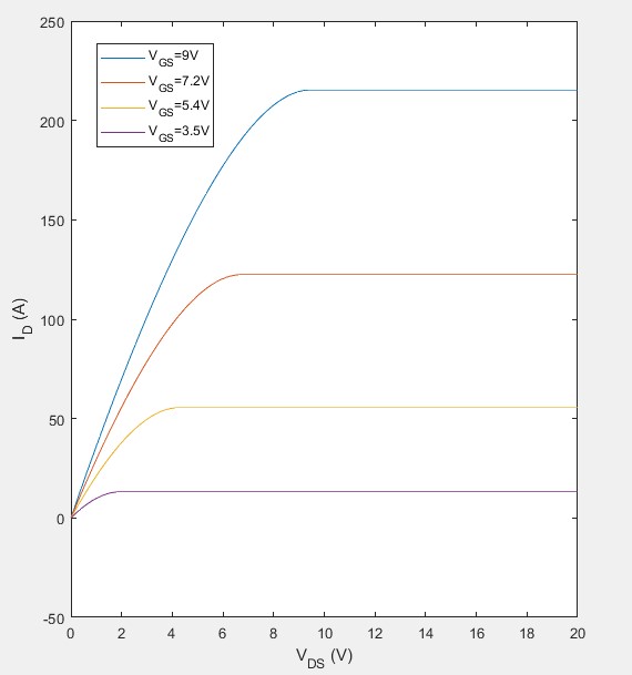
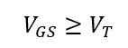
For all: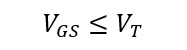
The drain-source is open-circuit: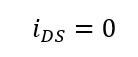 For all:
 The source-drain current is given by:
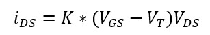
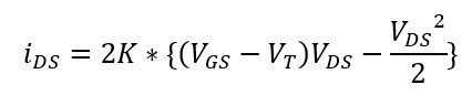 For small Vds, the square term can be neglected and response is approximately linear:
 For all Vds ≥ Vgs – Vt, the current saturates at a fixed value, given by substituting Vds = Vgs – Vt:

“What is the distribution of electric field, why at pitching-off it still conducts current, derive the expressions”. All these are extremely interesting questions to take up, but as far as engineering is concerned it won’t help design the circuit any better, so we don’t mind answering them in free time.
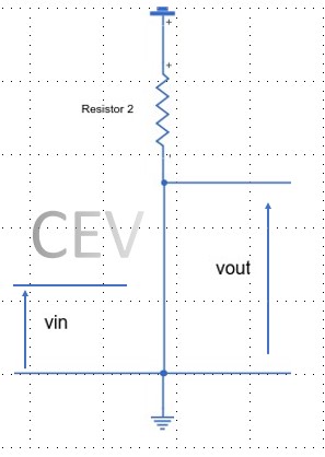
The most repeating circuit pattern of our Electrical lives, we can’t trace anything down to something more fundamental than this. Right here we saw for the first time the gate and the amplifier. Let this pattern dissolve in our blood, imprinted in our DNA, memorized in our brains and printed on walls of our heart. Well, that’s how fundamental it is. 😂😂😂

Before directly jumping to equations, let us first build intuition of how this circuit will respond to different applied input, which will allow us to flow through equations smoothly and swiftly.
So, what we need to imagine is the response of the circuit for different applied inputs.
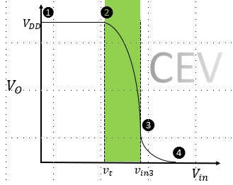
- For some applied value of drain voltage Vdd, we begin increasing the gate voltage slowly. As expected, until it reaches the threshold point, drain and source remains open circuited. Current through drain resistor is zero and hence output voltage equals Vdd.
- As the threshold potential is reached, the device just develops the so-called n-channel. Notice the current will just begin to flow and DS voltage will thus start dropping. Since the excess voltage is still smaller, and the DS voltage is sufficiently large to drive the MOSFET into the saturation region.
- If we still increase the gate voltage then excess gate voltage would be too much for the DS voltage to keep the MOSFET in saturation region. With increasing excess voltage, the channels widen, dropping the resistance, increasing the drain to source current and thus dropping the drain to source voltage, and at one point DS voltage is lower than Vgs – Vt and the MOSFET enters the linear region. (often called triode region)
 Notice we understood the operating characteristics is reverse order. To visualize in terms of how the MOSFET operating point moves on the operating characteristics will give more better idea.

At 2, the device just turns on and large value of Vdd immediately drives the MOSFET into saturation up to 3 where the MOS starts entering the triode region. Large dropping the DS, thus the output voltage to a very small value.
Mathematically:
Applying KVL, we have:
![]()
- For region 1 to 2:
![]()
So,
![]()
Hence,
![]()
2. For region 2 to 3:
![]()
Current saturates at: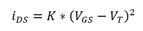
Thus, we have:![]()
Parabolic drop confirmed.
3. For region 3 to 4:
 Current should be given by equation:
 Thus, we have:
 A rather useless relation. 😀😀😀
MOSFETs as GATES:
We know that any kind of combinational logic can be implemented using three fundamental gates namely NOR, NAND and NOR. How to use this circuit for a NOT operation is quite evident from the transfer curve itself.
For small input voltage range, the output lies in range of some high voltage level, representing digital high logic.


For a range of high input voltage range, the output drops down to a range of small voltage levels, representing a digital low. So, all we need to do is to set Vdd and strictly define the input and voltage range for low and high logic., and we are done, we have got an inverter (NOT).

MOSFETS as Amplifiers
We have seen the requirement of a man-made device called amplifier to obtain a crucial signal manipulation, called signal amplification.
Amplifier in most general way could be called a source of energy which can be controlled by some input. Anyways there may be many more ways to look at amplifier, for example the earlier description of a transfer function block. More specifically this fits better into what we can call a dependent source. Before we understand what is amplifier let us understand what is not an amplifier. So, the element to be first excluded is a potential transformer. Though we can have a voltage amplification (step-up) we also have the currents transformation in inverse proportion so that power remains constant, similarly current transformer, a resistor divider, a boost configuration, etc. in which we have no power gain couldn’t be called amplifier. On the other hand, a MOSFET or a BJT appropriately biased, an op-amps, differential amps, instrumentation amps all are collectively called amplifier. Because we have a power gain at the output port wrt to an input port.
With one port as output and one input and third of course power port, theoretically speaking we can have at max 4 combination. Namely, we can have a current or voltage source at output, and we could have voltage or current control at input.
Any device for purpose of amplification invented in past or been invented or to be invented in future will fall in any one category.
The two-port theory becomes of immense utility, to easily describe different amplifiers in different matrix form, like Z-parameter, Y-parameter, h-parameter and g-parameter. We are constrained to not describe the theory in full detail; however, we will be building insight and motivation to study them.
We will use the same trademark configuration to do the amplification too. Isn’t this ground breaking? We had already built fundamental block for digital systems, and now we will again be using the same circuit for amplification which is of course an analog block.
So here it is:
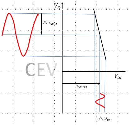
Remember, we didn’t talk about the region between 2 -3 when we studied this circuit acting as an inverter. We strictly worked in 1-2 or 3-4 region only.
 The transfer functions in 2-3 region as previously computed is:
![]() Though output voltage is proportional to input voltage, but nowhere close to linear. Remember what we have and compare it with what we wanted:
Though output voltage is proportional to input voltage, but nowhere close to linear. Remember what we have and compare it with what we wanted:
And here is the greatest revelation as the legends in this field had described for decades.
“The input signal is constrained such that the circuit approximately gives a linear response.”
And the revolutionary constraints are:
- Giving a DC level shift, to drive the MOSFET in the saturation region, popularly called biasing voltage, and
- if the input signal is small enough the transfer curve is much close to a negative sloped straight line, which is in fact linear amplification.
 If we zoom enough, here is how the amplification would look like. Notice inversion is there but a good linear amplification is also achieved.
We can also show that using the equation below that for small changes in input voltage indeed cause a linear change in the output voltage.
![]()
For,
We have,

So, we now comprehend the design problem of the amplifier as selection and operation at biasing point to get the best possible linear amplification for a given gain requirement.
And that’s a wrap. From here on we go on learning cascading amplifiers as one unit is not always enough to give desirable gain, which leads us to study the effects of stray and coupling capacitance which becomes especially troublesome when dealing with high-frequency signals, which then leads us to something called differential amplifiers, operational amplifiers, and as already describe we eventually take off from here.
All of this would be no so much use unless we also consider the energy consumption. Why it becomes so important can be understood by walking through some numbers.
Consider an inverter gate is build using the exactly as we have described.
For SMD MOSFETs of today’s technology, typically
K is 1 mA/V^2, Vt =1 V, Vdd we take 5 V (TTL Logic), and let low logic at the output is defined between 0-0.2 V
When gate is OFF, high level at input and low level at output:
![]()

Power consumed by circuit is:

For order of 10 million of them:
![]()
This very rough approximation of power consumption is not at all pleasant to see for 10 million inverters in days when processors are reaching the range of 4-5 Billion of them.
We would require a dedicated diesel-generator set for one 200-gm machine. Of course, we do something about it, that’s why our laptops could be powered by a 60 W Lithium battery. The solution is quite a creative one. They call it CMOS (Complementary MOS).
In order to have incredibly high resistance, when the gate is off and very small resistance when the gate is on, a PMOS is used to replace the resistor. PMOS transistor has exactly the same operation as NMOS, except it is open-circuited for the high level at input and short-circuited at a low level at the input. Also, Vdd has managed to reduce to 3.3 V to reduce power consumption.

We didn’t learn all of the stuffs by sitting down and just glaring at MOSFETs. The entire credit for vivid imagination and connecting the dots goes to numerous books, all the lecture series, few research papers, beloved Wikipedia and all the awesome discussions we had with our friends.
We are thankful to a Lecture Series on Fundamentals of Digital and Analog Electronics, 6.002 MIT OCW by Prof Anant Aggarwal, two 40 lectures series by NPTEL on Analog Electronics by Prof Radhakrishnan, an introductory lecture series on Semiconductor Physics and Devices by Prof D Das IISc B, Basic Electronics Course by Prof Behzad Razavi of Princeton University. This article is result of rigorous brainstorming of ideas, concepts and insights gained from all the above-mentioned sources and then making our own speculations.
Important revisions are yet to be made.
Keep reading, keep learning
Team CEV!