
Introduction
Multivibrators
Understanding the Circuit Elements
Battery
Voltage
Ampere
Ampere-Hour
Electronic Switch MOSFET
PINS
Physics in one-line
Circuit Diagram
Datasheet: Max Ratings
CD4047
PINS
The Astable Mode
Calculation of value of external R & C
Circuit Diagram
Datasheet: Max ratings
Three winding transformers
Turn Ratio
Filters
Choke coil
Capacitors
Final Circuits and demonstrations
Conclusion
References
In the previous blog “Inverter Circuits: The Basics”, we have begun with the very raw idea of DC to AC conversion and methodically we developed our basic circuit for obtaining a typical square waveform having power frequency from a constant voltage DC source.
The circuit was like:

We have understood the working of the circuit. Now for the purpose of practical implementation, all we require is the triggering circuit for the two MOSFETS at required frequency, proper dimensioning of the elements to check the reliable and safe operation, and also a filtering circuits to couple the load with our inverter circuit.
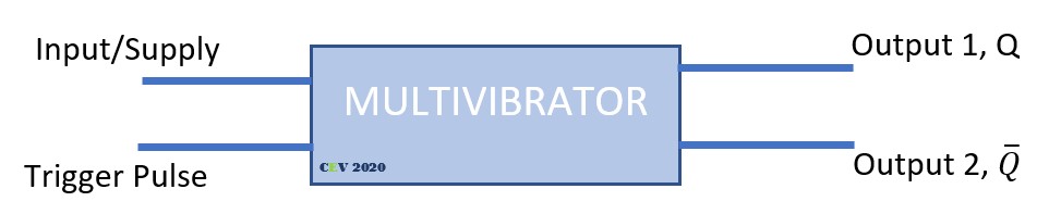
Let us introduce an exciting new class of electronic instrument…
Multivibrators
Multivibrators forms a wide class of electronic circuits and deals with two states (namely high and low) in different possible ways. Generalized diagram of a multivibrator:
They are a total of three kinds:
- Monostable Multivibrators: this sub-class is stable only in one of states, say high (1). So, once triggered by some external signal then the circuit enters into its unstable state i.e. low (0) and returns back to its stable state 1 after some pre-fixed time-period. Example of these types of circuits are delay generator, timing circuits, etc.
- Bistable Multivibrators: these circuits are stable in both the states (1 & 0), so if multivibrator is in high states and if triggered by some external signal its state changes to 1 and remains 1 until the next trigger. In simple words an external signal just flips the current state of output. Example of these types of circuits is flip-flops.
- Astable Multivibrators: they are unstable in both states, thus if you give trigger/supply to them the keep on oscillating between the two states indefinitely. They find extensive use in timers and oscillators.
We are only interested in astable multivibrators, for generating the timing pulse for biasing of the MOSFETS. There is a great range of IC that gives this mode of operation of continuous oscillation on a single trigger, the most popular of all ICs is timer LM555, in 4000 IC series we have CD4047, CD4049, CD4093, etc.
Understanding the Circuit Elements
Understanding the working and principle of a system comes under physics or pure science domain but realizing those systems by considering the real-world parameters and the effects is what engineering is all about. Element dimensioning, suitability, economics and all those things which come into picture when we try to turn a diagram drawn piece of paper into a real system to transform lives, is an engineering task. For example, working of an Induction motor is a physical phenomenon, but to utilize these machines in such large numbers littered beyond the horizon is only made possible by what we call power system engineering. So, there is a line where the physics ends and the engineering begins.

For an electrical system, it is the task of an engineer to take care of the parameter to be maintained under specified limits- voltage level to check dielectric breakdown and current level to check the thermal breakdown. With this background let us start exploring the circuit elements required in for our inverter.
Battery**
Voltage level, ampere-hour rating, max current rating
Electronic Switch MOSFET
The MOSFET we are going to use is the power MOSFET, modified specially to carry larger current, unlike usual low-power electronic circuits.
The device is identified technically as IRF540, n-channel 100V-0.055 Ohm, 22 A, Low-gate charge Power MOSFET, explained later.
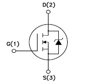
PINS:
It is a three-terminal device numbered 1, 2 and 3 as given:


The pins 1, 2, 3 are gate, drain and the source terminals.
Physics in one line:
MOSFET stands for Metal Oxide Semiconductor Field Effect Transistor, it is a voltage-controlled current device. The structure of the device is such that on the application of voltage at gate terminal a channel between the drain and source is formed which doesn’t exist earlier.
Without and with gate voltage:


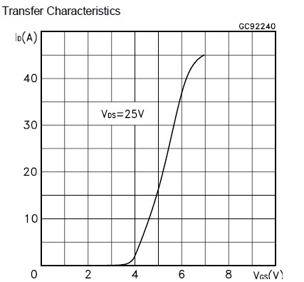
If you apply voltage at the gate terminal then for some voltage across drain-source the current begins to flow from (2) to (3). The more the gate voltage larger is current at a given drain-source voltage, which saturate at some point. Graphically:

DATASHEET
As earlier stated, after the physics we now have to look at the engineering part. This MOSFET has a limit on all of which can ve referred from the datasheet.
MAX RATINGS: 
Did you noticed the things written along the name of device? Here is what all that mean….

From the output and transfer characteristics it can be concluded that we should strictly restrict the gate source voltage between 4 V i.e. Threshold Voltage to 5 V for saturation current less than 22 A.
In the gate circuit let Vgg the supply voltage be 5V, Vgs be 4 V in on-state and Igs as 10 mA thus the value of resistance in the gate circuit for a given gate excitation voltage. (Refer datasheet)
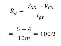
NOTE: Precise calculation for Ig is still not clear. The team thinks that maximum allowable gate charge and the pulse width has to be taken into consideration to calculate the maximum current that should be limited by the gate resistance. If you can contribute, please contact us.
CIRCUIT:


In the circuit during on-state, the forward resistance between the drain-source is given, thus depending on the Vdd and load resistance the current will flow which should be less than 22 A at 25-degree Celsius.
FUN FACT: It is amazing to know that the device MOSFET is no 1 manufactured electronic device in our entire history with 13*10^12 billion units sold by 2018 since 1964. 🤐🤐🤐🤐

Source: Wikipedia https://en.wikipedia.org/wiki/Electronics_industry#List_of_best-selling_electronic_devices
Check out which devices have been the top-selling product since their invention.
IMP HANDLING CARE:
Handling of MOSFET is little bit strenuous job, because it is a delicate device. If the gate, source and drain terminal are not shorted then there is possibility of static charge accumulation at the gate terminal hence forming enough electric field to puncture the ultra-thin silicon-dioxide layer, leading to permanent failure of MOSFET.
- Ground yourself when handling MOSFET.
- Keep the three-terminals shorted until plugged into the circuit.
- Voltage should be applied only after all terminal are connected to the electrical circuit.
The next thing is the pulse generator circuit for proper switching of the MOSFET 1 and 2 to obtain square wave of 50 Hz.
CD4047B
Introduced in the multivibrator section, we are going to use CD4047BE CMOS Low-Power Monostable/ Astable Multivibrator for the generation of required gate pulse.
PINS:


Datasheet describes the 14-terminals of CD4047BE with nomenclature and function of device as listed below:
Cleary we are interested in the Astable mode of operation as the gate pulse required is oscillatory with a 20 ms (1/50Hz) time-period.
The Astable Mode:
Again, datasheet according to the internal circuitry gives the terminal connection.

Calculation of value of external resistance and capacitors:
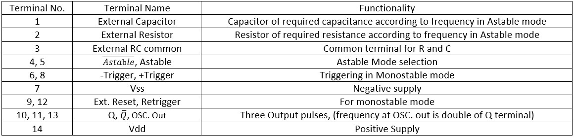
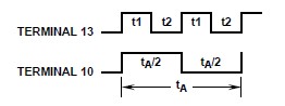
In the table above the time-period of pulse available at the pin 10, 11 is 4.40*RC seconds. This Q (pin 10) would ve the pulse input to the gate terminal of MOSFET M2 so that the positive square waveform appears across load. In the next half time-period Q will e low thus Q var (pin 11) connected to the gate of MOSFET M1 will e high and hence negative waveform appear across the load.
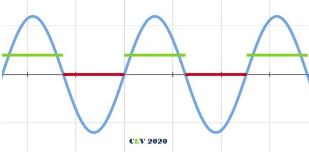
Assuming that we manage to get the sinusoidal output, the Q pulse and the load voltage waveform will look like:
The required frequency for voltage is 50 Hz, time-period of which is 20 ms, which also becomes the time-period of the pulse Q.
Referring the datasheet, the typical values of resistance and capacitance at which the multivibrator CD4047 produces pulses with greater precision, the value we chose are 45 kΩ and 0.1 μF respectively.
Circuit Diagram
Considering the pin connections, the circuit for the gating of the MOSFET using CD4047E can be obtained as given. The output pins 10 and 11 should be given to the gate terminals of any of M1 and M2 device.
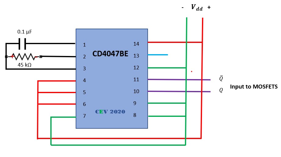

CD4047 being operated in Astable mode, R = 45 kΩ, C= 0.1 uF, Vdd = 12V
NOTE: The voltmeter measures RMS value and the waveform is pulsating DC, peak value has to be considered while calculations.
A visual illustration of pulsating waveform for R and C as 330 kΩ and 0.1 μF:
DATASHEET: MAX RATINGS
For different supply voltages the sink current and source current ratings are indicated as follows. The pulse voltage can also be experimentally determined for given supply voltage.

Thus, for obtaining required gate source voltage pulse, required value of resistor can be connected to interface CD4047 to the IRF540.
NOTE: The current limiting resistor calculation has still to be verified by considering the gate pulse requirement of MOSFET.
Three winding transformers
A three winding transformer is five terminals device as opposed to normal 4 terminal where we have two primary terminals and two terminals on the secondary side.
The basic transformation equation for two winding transformers, was:
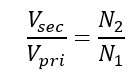
Where Vsec and N2 are voltage and turns respectively on the secondary side and Vpri and N1 for primary side.
In this case of three winding transformer this same equation is applicable on individual coil on primary as well as both coils combined.

For individual coil:
Here Vpri is voltage across any one of the primary coils. The transformer is rated as 12-0-12/240 V, 5A.
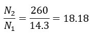
Hence putting the values, calculated value of turn ratio is:


a.) Measured Voltage across one coil for secondary being excited by mains supply
b.)Measured mains voltage on 21-03-2020 @18:30 HRS
So, actual turn ratio is:
For both coils combined:
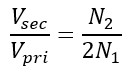
According to the given ratings, calculated primary voltage is:
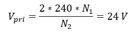
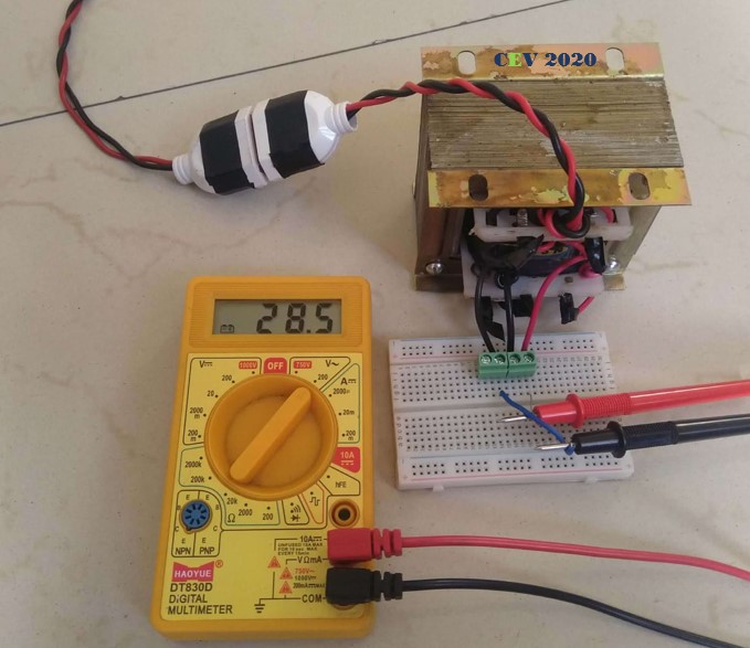 Measured voltage across both the primary coil
Using the turns ratio obtained in previous measurement, actual primary voltage is:
Which is verified by the voltmeter readings. So actual turn ratio is 18.18.
Filters
Choke coil
********
Capacitors
Capacitors are among one of oldest device used so widely in electrical circuits. Their characteristics can be utilized in numerous ways. In DC circuits they act as voltage smother by filtering out ripples (rectifiers), in radio technology they are used for tuning, in industries like automobile and aviation- they are utilized as emergency energy storage banks, in power system they are utilized for power factor improvement resulting in power and voltage regulation, and here we will use it in AC circuits to the block DC voltage.
The equation governing the behavior of capacitor in DC/AC circuits can be easily understood using some textbooks, here we will consider some practical application points.
Now the most important parameters of capacitor are its capacitance, its maximum operating voltage ratings and maximum reactive power handling particularly for high-voltage and power applications.
Capacitance value of 1pf ceramic capacitors to 50,000 uf Electrolytic type to 10F supercapacitors, with different operating voltages are commercially available. Depending on the requirement different capacitor technology can be opted. Consider this insightful graph from Wikipedia which helps in determine the capacitor type for a given requirement.
 Photo courtesy: Wikipedia
These commercially available capacitors are broadly divided in two categories:

- The polarized capacitors: These are polarity dependent and exclusively used for DC applications.
- Electrolytic types: gives advantage of small size and stability for relatively larger C (few uf to thousands uf) compared to unpolarized ceramics-type. Application in DC voltage smothering, etc. Also used in AC fan motors, how. Can you answer???👴👴👴 (0.1 uF – Thousands uF)

IMP: The terminal marked negative should always e connected to the negative polarity of source.
2. Supercapacitors: most versatile category. With higher capacitance, they find applications in the field of electronics (to power memory during power cut-off), transportation, renewables, etc. Though the typical capacitance of single unit is higher but it’s working voltage is mere 2-5 V, so numerous cells are connected in series to obtain the required rating.

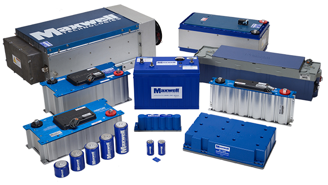
Photo courtesy Internet
2. The unpolarized capacitors: These capacitors have no polarity specific terminals. Hence used in both AC and DC applications.
a.) Ceramic type: ideal for smaller capacitance and for wider frequency (specially high) spectrum. Oscillator tuning, HF applications. (1 pF – 0.1 uF).
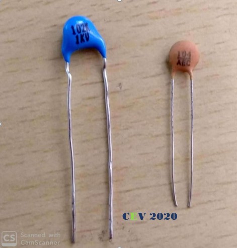
The meaning of 102 is 10*100 pf and 104 is 10*10000 pf. First two digits are the values and last is the multiplier and value come in pF.
- Film-type: More popular in high-voltage and high-power applications like snubber circuits, etc.
 Photo courtesy Internet
As far as general projects are considered either ceramic or electrolytic is preferred choice according the capacitance required.
Another important class of capacitors is the capacitors system employed in power systems, which goes far beyond off-topic to be discussed here. However, for purpose of mere excitement and spark curiosity in the readers interested in electrical field this particular stuff, here is view of those massive capacitors systems:
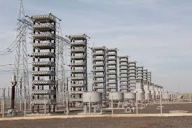
General Electric power factor compensation utility for power grids
Notice that the tiny ceramic capacitor and these megs-structures are also defined by same physical equation Q=CV and all others, and see how engineering has made them strikingly different. A physicist can only give us those equation but it’s the job of engineers to pump life in those dead equations to build some stunning things.

The last circuit:

The actual test circuit working at 50 Hz:

Visuals of circuit operating with 330 kΩ resistance in CD4047:
The Inverter Family😇😇😇:

Conclusion
Making the circuit work as expected was not the final aim of the project which we failed also as of now because of shortage of resources due to corona virus outbreak (low rating battery, choke coil, etc), thus not able to test our circuit on actual AC load.
But the core objective and higher purpose of the initiative which was to develop the critical thinking to build a concept of circuit to obtain desired results for a given set of initial conditions, honing skill to be able to select appropriated element from numerous choices available by considering the suitability, economics, etc., working out the circuit parameters by referring the standard datasheets and be able to work in team was surely achieved to satisfactory level.
References
Drive link to datasheets, important lectures videos and notes, etc:
https://drive.google.com/drive/folders/1fVLofMnjowNTGhpMEXaqG7IFt_WrT4v4?usp=sharing
Meanwhile the documentation of project was done in respect of the man Richard Feynman on whose vision CEV hang so tight:

Science will do help us win over this corona thing, just as it has helped humanity fight influenza and whatnot, till then hold strong and keep believing.
Keep reading, keep learning!!!!!
TEAM AANTARAK, CEV
Anshumaan S Jhala | Chitturi Vamsi | Rakesh Dhadavi | Nitin Patel |Shayam | Rahul Kumar
Special Contributor: Vartik Srivastava
Great Deal of hardwork man!!