
A controlled buck converter finds its application in innumerous platforms. It elegantly executes the mobile fast charging algorithm, MPPT algorithm in some Solar modules, robotics, etc. with optimal desired performance. It is elementary power converter, used as a power source for other electronic equipments like microprocessors, relays, etc.
One can jokingly say it the 1:1 auto-transformer of DC electricity world.
Buck converters which are also known as step-down choppers, are much ubiquitous hence it becomes very handy to have a design scheme, tested procedures and simulation models to fastly and accurately build a ready to deploy DC Buck converter. We will not describe in great depths the working as the principle of operation can be found in any standard power converter textbook, however, in this blog we wish to present a step by step guide to design a buck by taking into account all important practical considerations.
General Schematics

The circuit operation can easily be understood by sketching the waveforms in two states, i.e. when the semiconductor switch is triggered and when it is not triggered.
ON-STATE: Inductor current rises linearly with time as voltage source get directly applied across the inductor and load.
OFF-STATE: Inductor current decreases linearly as the circuit gets short-circuited by the forward-biased diode, which allows for current free-wheeling.
The average voltage applied is a function of time for which the semi-conductor is turned on and turned off, which is indicative of the duty cycle of the pulse generator.
Specifications
The first thing we require is all the desired ratings and performance of the buck converter. These specifications ultimately determine the device parameters, which will give the desired operation. Consider the sample case in which we are operating a constant power load with a variable input DC voltage source, for example a solar module.
Ratings:
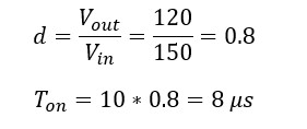
- Input: 150 V- 400 V
- Output: 120 V
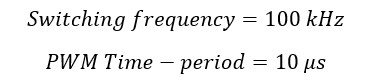
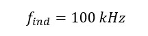
- Switching Frequency: 100 kHz (typical for choppers)
- Load current: 50 A
Performance Parameters:
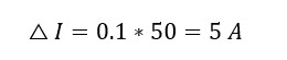
- Ripple (P-P) in load current: 10%
- Ripple (P-P) in load voltage: 5%
- Max Load Power support: 25%
- Max Voltage drop during support: 10%
- Backup duration: 10 ms
Keeping in mind these desired performance parameters the ratings of the various elements will be decided.
Circuit Element Rating Calculations
Inductor
The value of Inductor determines the ripple in the load current. Having large ripples in load causes poor performance of DC load, like lights will flicker, DC fans will produce pulsating torque and noise, etc.
Since varying the duty-cycle will result in different turn-on and turn-off time thus causing varying ripples. All we have to do is to do a trial and error procedure to find the value of L to get ripple below permissible limits under all possible cases:
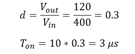
Test case 1: Vin = 150 V; Vout = 120 V
For peak to peak ripple current of 10%:
Now inductor equation during on-time is:

From circuit:

*Assuming load voltage remains almost constant during the entire cycle
So,

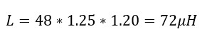
Now here comes very crucial part. The theoretical value of inductor has been calculated, but the important things is, in the real environment we always need to overrated our circuit elements to accommodate the uncertainty of the real world. If we are designing a commercial product there is a very tight margin for these over-ratings. That’s why all the gadgets are always rated to operate in a specified environments, like temperature, moisture, etc.
It is good practice to keep a safety factor of 25% for operating temperature changes and 20% for derating of inductor coil over time:
Extreme Test case 2: Vin = 400 V; Vout = 120 V **Worst case calc
For peak to peak ripple current of 10%:
Now inductor equation during on time is:
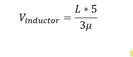 From circuit:
![]()
*Assuming load voltage remains almost constant during the entire cycle
So,
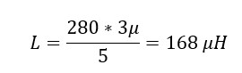
Again, keeping a safety factor of 25 % for operating temperature changes and 20% for derating over time:

Now since worst-case requirement doesn’t meet previous case value thus the inductor value should be updated to at least 252 uH.
We must also verify the ripple current requirement at met for input voltage in between 150 V and 400 V:
Random Test case 3: Vin = 250 V; Vout = 120 V

Hence verified!
Now max current through inductor:

Also,
So finally, inductor ratings are:
![]()
Parameter met:
- Ripple current is less than 10% for all cases.
Semiconductor Switch
Peak Reverse voltage occurs under off-time:
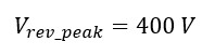
Considering safety factor of 30%:
Peak current would be same as inductor current, and taking safety factor of 25% and 30% for spikes due to stray inductance and temperature rise;

So, the semiconductor switch ratings are:
![]()
*RdsON should be as low as possible.
*Now since the reverse peak voltage is less than 600 V so a MOSFET can be employed, however if gating loss has also to be considered than IGBTs would be preferable.
Diode
Diode will also be subjected to same voltage and current ratings as that of the MOSFET.
![]()
*In addition, care must be taken to select a diode will high frequency operating capabilities in order of 100 kHz.
Capacitor
The high-frequency ripple present in the inductor current will be bypassed by the capacitor, as its impedance varies inversely with frequency. However, in an ideal capacitor, there is always some series resistance with leads to ripples in voltage across the C terminal, inturn the load terminal.
- Effective Series Resistance (ESR) Ratings:
A ripple of less than 2% is desired in output voltage, so:

Since ripple in load voltage is largely caused by the series resistance,

Parameter met:
- Load Ripple voltage of less than 2% is obtained for all cases since 5A is the maximum ripple in the current.
Moreover, this charged capacitor discharges to meet the load current for a small duration when supply is lost or small increase in load. This same principle is applied in many electronic gadgets like PC, laptops, etc to bridge the power loss during switching from mains supply to back-up power.
2. Capacitance value:
For a load change of 25% a corresponding load voltage dip of 10% and a backup time of 10 ms is desired.
10% Dip in voltage:

25% change in load is:
![]()
This power should be supplied by the capacitor and thus will discharge it:

Making critical approximations, which we all engineers so good at:

Capacitor voltage with 30% safety factor:
![]()
So:
![]()
Parameter met:
- The load voltage drop of less than 10% is obtained for 10 msec for a load increase of 25%.
Simulations
**MATLAB MODEL

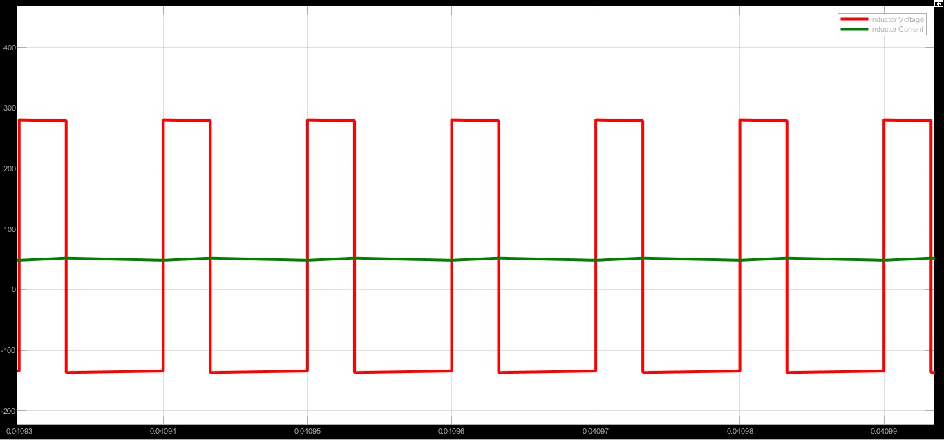
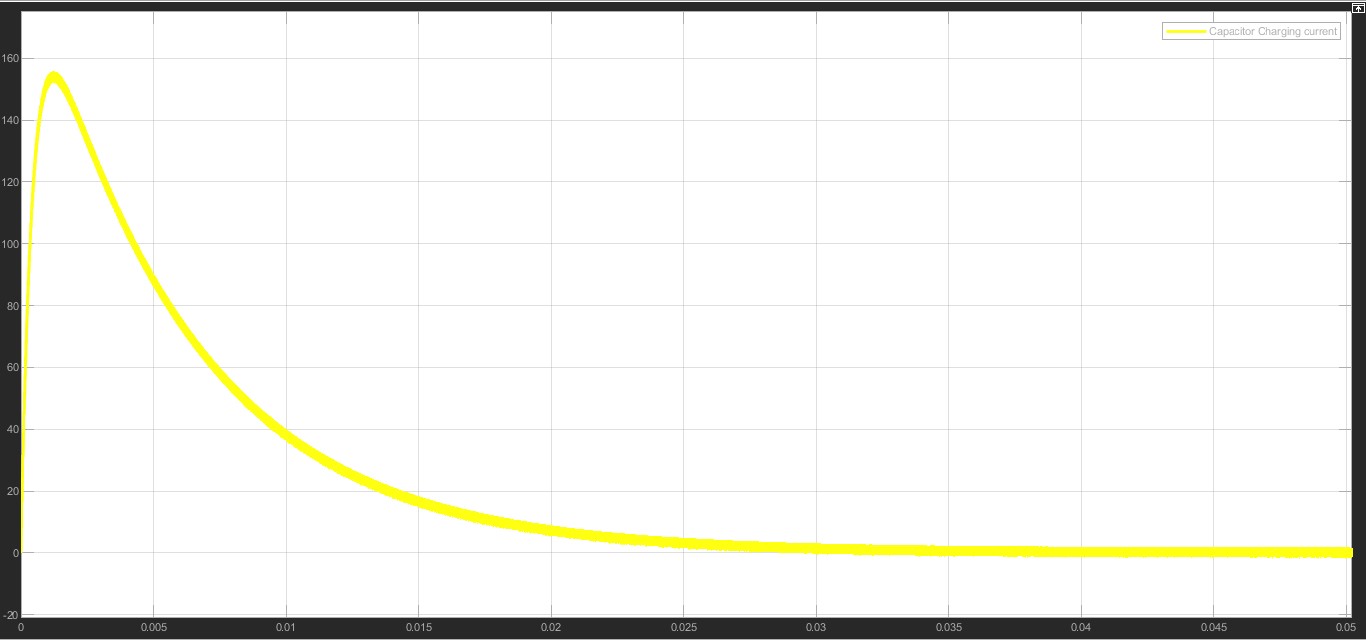
Displays show the result for 400V input, notice 120V output and 50 A load current.
Waveforms
- Inductor voltage and current:
2. Load voltage and current:

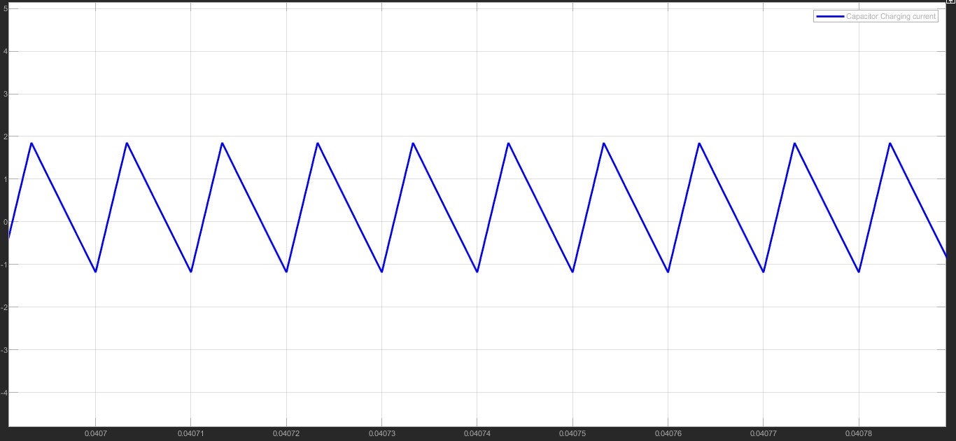
3. Capacitor current transient:
4. Capacitor steady-state ripple current: ripples bypassing
5. Diode Voltage:

Controller Design
Now comes the most elegant part of designing a buck converter, modelling a buck to understand and predict the performance in a closed-loop operation.
Like any linear control system, we first need to identify the input and the output. Here we have reduced the buck converter to a simple RLC circuit to check the response of the system for various input of duty cycle:
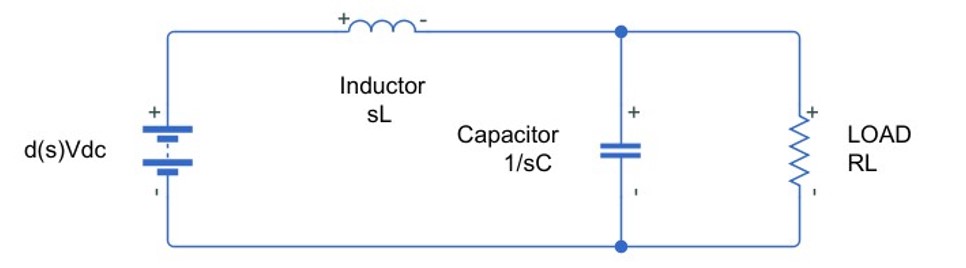
The transfer function model obtained for this open-loop system is as follows:
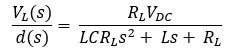
Where:

Now as per one’s convenience we can either go with root-locus analysis or with the frequency domain analysis.
We know from control theory that by obtaining the bode-plot of an open-loop system we can say a lot about the closed-loop operation of the system. We can comment on the stability, relative stability as well as with little speculations we can also comment on the transient response!!
We might have dived in depths of Control Theory, but we restrict ourself to buck only. Probably, we will find some other fine day to do that.
Obtaining the bode-plot for above open-loop transfer function by running the following code in SCILAB:
s=poly (0, ‘s’);
p =          960/ (2.4 +0.000252s +0.0000063s²);
p= syslin (c, ‘p’);
clf ();
bode (p, 1, 5000)
The bode plot for the uncompensated system:

From bode-plot it can be directly concluded that the close loop system will be unstable as the phase cross over frequency is less than the gain cross-over frequency.
By the conventional steps, we need to first use a lag compensator to make gain-cross over frequency less than the phase cross-over frequency.
- Adding a lag-compensator around the gain crossover frequency of around 2000 Hz.
- Adding lag compensation at around 2000 Hz is given by:

Bode-plot for the lag compensated system:

It is evident that now the close-loop system of this open system will be stable but the margin of stability is less.
So, using a lead compensator to provide the required phase margin at the gain cross over frequency, i.e. around 2000 kHz.
TF for required lead compensation should be:
![]()
A well-compensated and stable system:
*If desired more lead compensation can be provided according to the design specs.
The final open-loop gain becomes (assuming unity feedback system):

Now op-amp can be used to make these lag and lead compensators, and using analog electronics duty ratio generation could also be done. CEV ask for apologies to not do that today.
The Last Words
Team CEV’s purpose of posting technical blogs is to help out some of the folks who have been completely or partially saddened by the conventional ways of teaching and have been extremely demotivated to keep their interest in these kinds of stuff which is otherwise so rich and interesting.
We are aware that the system has failed us to boost and strengthen our interest in the subjects. 1/7 th of humanity shall not be devoid of fun and joy of falling in love with the subjects, by no fault of their own.
This is simply not acceptable to CEV.
We are not here to just do casual criticizing about the things rather we understand the severity of the situation and quiet boldly take the ownership to undo the damage, even by a fraction of %.
We believe that people in light of their own personal insights can put out things is much appealing and fascinating way, unlike the usual exam-focused, dull and dead description of things. We intend to rekindle the fire of curiosity and interest and help keep the learning spirits of our generation of student community real-high.
Cheers!
Team CEV.
Featured Image courtesy pixabay.com.