The manufacturing sector has been on the ventilator for a long time……
Despite a demand of 1.36 B we import quite a large portion of the products employing moderate to high-level technology, from electronic toys to smartphones to high power Induction motors of Indian Railways Engines. We don’t have any airliner manufacturing except HAL, we don’t have chip manufacturing even though we are land of powerful the Shakti microprocessors. How much sadness this fact bring home to us!
Consider Solar Cell & Module Manufacturing industry.
We have a small number of solar modules manufactures who import solar cells largely from China & Taiwan paste them on a tough polymer sheet, use some power electronics and meet the large demand of India solar needs.
We have even much small solar cell capability, who import wafers, own some mega turn-key solar line manufacturing unit mostly set up by European Companies. You see, we have to be very precise in claiming what is ours and what is not.
We import 80% solar cells and solar modules and a domestic manufacturing capacity of only 3 GW for solar cells. -Source: livemint.com
In this blog let us at least critically understand what goes in the making of 21st century solar cell. And try to figure is that so hard, that we really need to import end-tailored billion euros turnkey lines to get the solar industry flying.
For good assimilation of the content, one needs to be familiar with a solar cell. One might answer the following question to get a temporary check-pass.
- How does charge generation, charge separation and charge collection phenomenon occur in a solar cell?
- What is meant by the short circuit current and open-circuit voltage of cell?
- Difference between the solar cell and solar module.
- On what factors does the form factor depend?
Notice the nature of the question, they are descriptive and have straight forward answers.
We don’t have here full degree of freedom to ask any wild question. For example, one cannot ask what would be voltage measured by non-ideal voltmeter across the photocell under no illumination, would current flow through external resistance in a not illuminated solar cell or a regular diode.
The reason is, from the engineering point of view we always study an abstract model of a solar cell or p-n junction. Physicists have very smartly built a layer over all the intricate things going inside the cell, we don’t care much about the exact phenomenon inside of the device, yet with the help of modified equations, we can deduce engineering relevant parameters like FF, Rsh, Rs, Isc, Voc, etc and can do clever things like MPPT, etc.
Similarly, using our conventional theory, one cannot explain the presence of intrinsic carrier at room temperature.
A pure silicon crystal has a bandgap of 1.12 eV, electrons on the other hand according to classical theory have thermal energy of kT (i.e. 0.026 eV or 26 meV). So intuitive physics would lead us to conclude that at room temperature there should be no electron in the conduction band. Still, at 25 degrees 10^10 electrons per cubic cm are available in the conduction band in a pure silicon crystal, called as intrinsic carrier density.
Think for a second how would you explain this paradox?
All these questions, wild or sober, can surely are answered satisfactorily (multiplying and integrating maxwell Boltzmann density of states and Fermi-Dirac probability distribution) but the point I want to highlight is that they really unfold the need of another kind of theory to explain, and let us reveal to you that is what the world knows as the quantum theory of matter.
Notice the power of our wild questioning, one correct question has simply enabled us to knock the door of mighty quantum physics. What a pleasure to discover for ourself the need for new theory, the theory which the world has been developing for the past 130 years.
On the other hand, if we think we are done with the p-n junction, simply-just by being able to describe the formation of depletion region and calculating the build-in voltage by a sweet formula without a taste of weirdness of quantum physics, then we should really reconsider our beliefs.
The flow
Ingot Growth
Wafer Slicing
Saw Damage Etch
Texturing
Emitter Diffusion
Anti-Reflection Coating
Front Contact
Back Contact
Firing
This blog won’t be really spitting out crude information throughout as it seems from the flow, rather it aims to induce self-questions in readers and thus provokes the reader to discover for themselves the tight constraint the solar cell manufacturing posses at every stage.
Now the first input is the silicon wafers. It itself takes a whole manufacturing industry, it has it’s own difficultly why India doesn’t have that, so we will not dive deep rather just walk through it until solar domain actually begins, you can even directly jump to Saw damage etch.
INGOT GROWTH
Silicon crystal falls broadly in two categories the monocrystalline silicon and polycrystalline silicon. Monocrystalline crystals contain continuous single crystal orientation.

Polycrystalline crystal, however, has much less regularity, and have many grain boundaries. The solar industry is always on toes to minimize the cost per unit energy produced as its competitor is the outlet in our homes, so it can’t afford at any stage a high price manufacturing technology.

Polycrystalline silicon is formed using the Siemens process, a faster and cheaper growth method as compared to Czocharalski, and float zone process for crystalline silicon.
Wafer Slicing
The next obvious step is the sawing out the wafers, evident from the ingot structure that the monocrystalline will be circular and polycrystalline will be square type. Slurry based sawing and diamond-based sawing are two popular techs, out of which diamond-based become much popular because it is fast and produce more yield as silicon dust produced is less.
No matter what techniques is used the roughness on the surface is way more than acceptable for the solar use or any (IC industry).

Pseudosquare shape to optimize the material requirement 
Saw damage Etch
Enough of the peripheral walks, now we are entering the woods, from here we are entering the solar manufacturing.
To smooth out the scratches and remove the surface contaminants caused by sawing, the p-doped wafers are treated with a strong hot alkaline bath, like NaOH or KOH. We can also leverage the non-uniform surface to increase the probability for light to enter the silicon but it’s avoided as any deep crack has a chance to develop into a larger hairline fracture as Silicon is brittle at room temperature and hence breaking cell in some time.
The alkaline solution dissolves the 5-10 um thick layer from both ends, resulting in very fine surfaces and a p-type wafer of width in the range of 170 um. Precise control of temperature, concentration and time is required in the bath for desired outcomes.
Texturing
If the surface is perfectly smooth the light won’t get any chance to re-strike the surface again. The greater the number of times the light is reflected by the surface the more chances it has to enter the bulk of the silicon. However, for adequately rough surface the light reflected from the edges have more chances to enter the silicon.

Image courtesy: pv-manufacturing.org
The process of saw damage etching and texturing only differ in concentration and temperature of alkaline. A much lower concentration alkaline is observed to yield pyramid-like structure over the silicon surface, which aids the cell to greatly reduce the reflectivity of the surface.
 Image courtesy: pv-manufacturing.org
A great amount of attention is given to tiny-tricky light management techniques. Using the principles of optics, the solar cell is optimized to somehow get the maximum photons inside (or increase the path length inside the silicon). These include Texturing, anti-reflection, back internal reflection, etc., in fact you would be surprised to know that attempts have been made by some companies to even texture the surface of fingers and busbars to divert the light falling on them towards the silicon, and like that.
Emitter Diffusion
The presence of the electric field is inevitable for charge separation as photons knock out the electron from Si atoms. Thus, next in line is the formation of the n-type region to develop a depletion region (p-n junction) inside the cell which assists in change separation.
The process is quite straight forward. We have a heated POCl3 gas inside a chamber and correct temperature and vapour density are maintained to allow the phosphorous atoms to diffuse into the silicon base.
The trick is how will one decide the doping density of the emitter layer and the thickness of it.
High doping density is desirable to have a good contact (less metal contact resistance) and low lateral series resistance as charges moves along the emitter, however higher doping density causes to decrease the bandgap of Silicon (as at extreme doping the crystals begins to become highly irregular, thus shrinking the band-gap) hence the blue light (high-frequency radiation) is not absorbed well, also recombination ( a type called Auger Recombination) increases in emitter leading to dragging down of the open-circuit voltage of the cell and hence the performance.
Now think about the thickness of emitter, ideally, the emitter should be narrow so that the time it remains inside the gas chamber is less and the process is faster and cheaper.
But if it is narrow there is a great chance that the metal will leach through it into the p-type directly shunting them, leading to extremely poor-quality cells.
Notice that every piece of solar cell development is a tight problem of optimization.
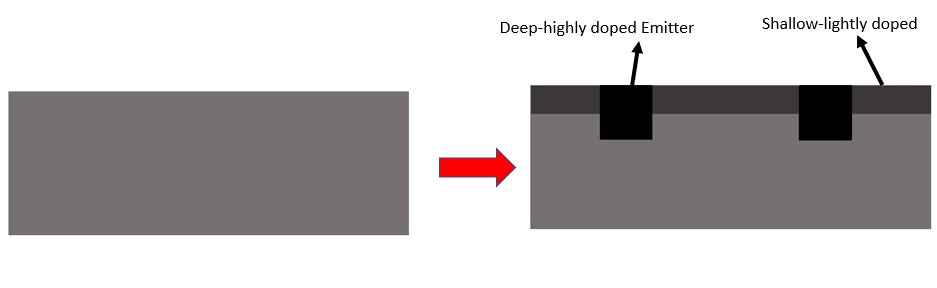
We require two contrasting qualities of the emitter, narrow and lightly doped for good light response and low recombination, and deep and heavily doped for good contact and low series resistance.
Selective Emitter is quite a smart way to accommodate both of them.
A shallow lightly doped emitter is formed first then by proper masking deep heavily doped contact regions are obtained.
Anti-reflection Coating
This is one more way to increase the probability of light to get absorbed in the solar cell. Using a Silicon Nitride coating the light is reflected back into the cell.
The process generally used is called PVCED (Plasma Enhanced Chemical Vapor Deposition).
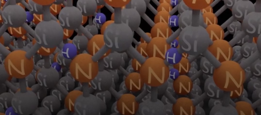 Image courtesy: pv-manufacturing.org
Silane (SiH4) and Ammonia (NH3) are filled in a chamber and excited by high-frequency waves. Obeying the rules of chemistry and fine-tuning the process an extremely thin 70-nm layer of Silicon Nitride is formed above the emitter junction.
The added benefit is that the hydrogen released in the process bonds with dangling Si atoms which otherwise would have led to increased recombination, anyways this process of filling the holes is called passivation.

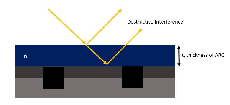
The way in which this anti-reflecting coating works is truly an elegant piece of physics.
They work on principles of interference. We know that rays of monochromatic light can interfere depending on the distance (optical) travelled, as it causes a change in phase. The famous Michelson experiment produced constructive interference if path difference was λ, 2λ, 3λ, whereas produced destructive interference for λ/2, 3 λ/2, 5λ/2, etc.
Magnified ARC layer
On similar lines, these 70 nm manages to produce a destructive interference of waves, thus suppressing the reflection from the surface and constraining the entire intensity to get transmitted.
For normal incidence the light travels twice the thickness of ARC, so for destructive interference, the optical path length difference between the two waves must be λ/2. Due to decreased speed of light inside higher refractive index material, the optical path length will increase by a factor of n.

Where n is the refractive index of ARC.
Now, solar radiation is not monochromatic, hence we can never obtain destructive interference for all the wavelengths for one thickness of ARC. Thus, the thickness is optimized for wavelength at which peak of solar radiation occurs, i.e. 2.3 eV (550 nm). Given Silicon Nitride has refractive index of 2, plugging in the numbers we get:

It is here from where we get the golden number of 70 nm, which is so popular in solar cell industry.
Front Contact printing
This is also one of the typical optimization problems in solar cell design.
For good ohmic contact (low contact resistance) the fingers must be wide, but for maximizing the amount of light entering inside the cell the fingers must be as narrow as possible.
Even finger spacing is a critical design parameter. Small finger spacing is desirable to keep the series resistance low, but it will lead in a larger portion of cell area to get shadowed by the front contact, again an engineering decision has to be made to optimize the net performance.
In fact, optimization constraint occurs in one more dimension here, the height of the fingers. One would like to have increased height to increase the cross-section for the current but again it would be limited as when the sun falls slantly the large shadow of these fingers would be casted if the height is large.
Same problem for the busbars too.
However, once the design is optimized the printing as easy as t-shirt printing. Making a mask and applying the paste and then drying.
Generally, a silver-based paste is used for the purpose.

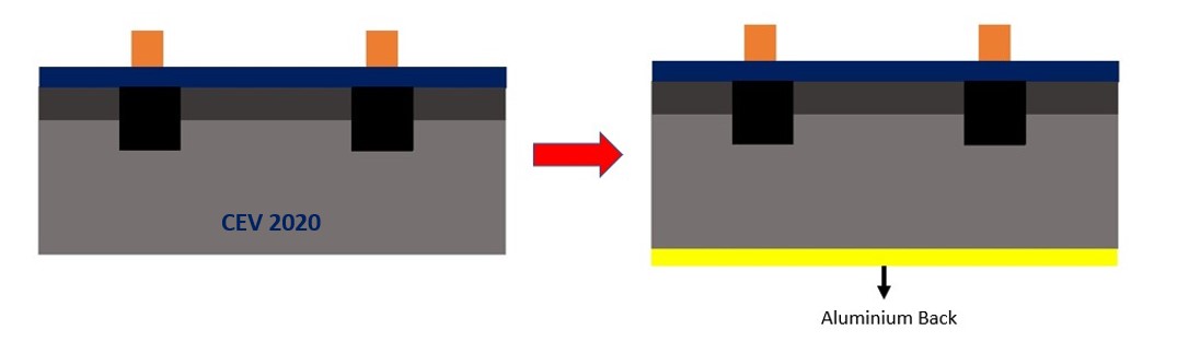
Back Contact Printing
Back Contact seems simple at first sight but like all the solar cell stuff it too poses optimization problems of its own. The Solar cell is supposed to operate in quite large temperature ranges.
Silicon has a lower thermal expansion coefficient than that of the metallic aluminium. If appropriate care of thickness of aluminium back is not taken then the difference in thermal coefficient might lead to intolerable bending of the cell, leading to even separation of contacts in the extreme case.
A layer of aluminium is developed on the back surface, the thickness of which typically lies in the range of 30 um.
However, this Al layer has an added benefit of what is called the back-surface field (BSF). Some of the Al diffuse into the p-type base and thus making it p++ type. The direction of the field developed to repel the minority carrier electron away from the back surface, and this also reduces recombination at back.
Firing
Technically called post-deposition high-temperature annealing.
Notice that the front metal doesn’t make electrical contact with the emitter. So, the cells are lastly sent in a furnace of accurately controlled temperature. The heated silver etches through the tough 70 nm ARC and makes just suitable contact with the emitter.
This process has to be very finely tuned if the temperature is not high or cell is kept in the furnace for small-time the contacts will not be firm and hence result in high series resistance. If the temperature is high or the time is more than the molten silver will breach through the emitter to base, thereby directly shunting the device and giving rise to extremely small shunt resistance and hence again a poor performance device.

Conclusion
The General Conclusion:
One can conclude for ourself that the manufacturing of solar cell is not so advanced as engineering quantum systems like manipulating Q-bits or fusion of atoms or replicating human brain, it is an arena of extreme fine-tuning and very precise control of temperature, concentration, motion.
The Technical Conclusion:
The solar cell is the best example of a most well-optimized system, in the real commercial scenario, it takes into account 30+ parameters.
It is also a standing example that little things in life matters and sometimes even more. Just like a team is only fast as slowest guy in the team similarly any engineering system is only efficient as least efficient component in the system, so nothing has to considered trivial or irrelevant or less worthy of attention, and it applies equally to life and non-living systems.
Some cool websites to learn and understand the solar cell in greater deaths:
1. pveducation.org
2. pv-manufacturing.org
Keep Reading, keep learning,
Team CEV!
Featured Image courtesy pixabay.com.