“Nothing vast enters the life of mortals without a curse.”
In 2020, Netflix released a documentary drama movie named “The Social Dilemma” directed by Jeff Orlowski which explores the rise of social media and the damage it has caused to society, focusing on its exploitation and manipulation of its users for financial gain through surveillance capitalism and data mining. According to recent estimates, approximately 3.8 billion people are active on social media worldwide which means that today more people are connected than ever through various social media platforms. Look around yourselves, which are the most visited Apps on your smartphones, you get to know how deep social media has penetrated our life. When asked about the impact of social media, creators said that they had never imagined to which extent their product would go on impacting the lives of common people across the globe. Social media did a fantastic job in helping people in their difficult times, it helped in searching the donor for organ donation, helped the needy to get donations, helped students to get free study materials online very easily, helped beginners to start cooking and there are endless examples of how social media has helped humans. But something has changed over the years. The world is changing at an unprecedented rate like never imagined before and that not in a good direction.
Earlier the social media platforms were used for sharing photos and videos and connecting to people. The Internet was simple at that time. Now social media platforms like Facebook, Snapchat, Twitter, Tiktok, Google, Pinterest, Reddit, Linkedin, etc. compete for our attention.
Today’s big tech giant companies are making their product keeping three main goals in their mind:-
1.) Engagement goal- They want to drive up usage and keep you scrolling on their platforms. They want you to scroll through their platforms as much as you can do. But the question is how do they do that, right? They do it by using the machine as persuasive social media actors. It is called persuasive technology. Let me explain by giving a reference to two studies that were conducted at Stanford University in the mid-1990s that showed how the similarity between computers and the people who use them makes a difference when it comes to persuasions. One study examined the similarities in personalities while another study examined similarities in affiliation. Research highlights of the study are below.
Research Highlights: The Personality Study:
Created dominant and submissive computer personalities
Chose as participants people who were at extremes of dominant or submissive
Mixed and matched computer personalities with user personalities
Result: Participants preferred computers whose “personalities” matched their own.
Research Highlights: The Affiliation Study:
Participants were given a problem to solve and assigned to work on the problem either with a computer they were told was a “teammate” or a computer that was given no label.
For all participants, the interaction with the computer was identical; the only difference was whether or not the participant believed the computer was a teammate.
The results compared to responses of other participants: people who worked with a computer labeled as their teammate reported that the computer was more similar to them, that it was smarter, and that it offered better information. These participants also were more likely to choose the problem solutions recommended by the computers.
2.) Growth goal- They want you to connect with your relatives, your friends, even strangers and make them your friends, explore various attractive locations, crave tasty food, invite more people on the platform for engagement, etc. for one and only one reason, You visit their platforms more and more. Let me give you some examples from your daily social media experience. There are two forms of interactions that take place on Facebook: active interaction (liking, sharing, commenting, reacting) and passive interaction (clicking, watching, viewing/hovering).
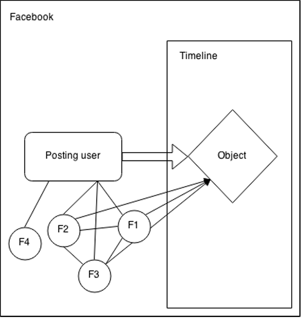
Active interaction: Whenever someone likes your post or vice-a-versa, it gives a sense of joy that they like us or we like them. It creates a loop for you and them to visit each other’s profile more often and chat which means you will chat with them on social media platforms and you visit more. You share memes with them, react to their stories, you react to their reactions and ultimately you end up spending more time on their platform. It also creates a rat race for more no. of likes which can affect mental health. The more you crave for likes, the more you are expected to spend time on social media figuring out how you can increase your likes and get recognition amongst your peers. Below is the excerpt from a study on “The social significance of the Facebook Like button” by Veikko Eranti and Markku Lonkila.
The figure suggests, first, that the relationship with the original poster of an object may have an impact on likes: We are more prone to like a post by a close Facebook friend than one by an acquaintance whom we have accepted as our friend somewhat reluctantly. Second, the quality, number, and network structure of previous likers are likely to affect one’s likes. This is probably even truer in the case of a sensitive or contradictory topic (e.g., a post on a political issue). Thus, if F1, F2, and F3 are close friends, F3 is more prone to like a post of controversial nature if F1 and F2 have both already liked it. Third, the imagined audience constructed subjectively by the user of the pool of all Facebook friends (some subset of F1–F4) is likely to influence liking behavior.
Passive interaction: Now remember when you were not talking with anybody, not reacting to any stories, not commenting on any post but still active on social media, what were you doing? You were seeing videos and simply scrolling through various posts, memes, videos, reels hoping for the one post that you may find interesting and can like or comment on it, isn’t it? How long it took you to find the post you wanted to see. Probably not too much, your social media platform did not take a long time to guess what you want to see, but the question is how? Adam Mosseri, head of Instagram might answer your question, “Today we use signals like how many people react to, comment on, or share posts to determine how high they appear in News Feed. With this update, we will also prioritize posts that spark conversations and meaningful interactions between people. To do this, we will predict which posts you might want to interact with your friends about and show these posts higher in the feed. These are posts that inspire back-and-forth discussion in the comments and posts that you might want to share and react to – whether that’s a post from a friend seeking advice, a friend asking for recommendations for a trip, or a news article or video prompting lots of discussions.”
3.) Advertising goal- When two people are connecting on the social media platform for free, it’s obvious someone is paying for it. A third party is paying for manipulation for those two, the other two, and every other person who is communicating through social media. We are in the era of surveillance capitalism where big tech giants are collecting a massive amount of data and collecting them at one place to show personalized ads to their customers and earn maximum money from advertising. It’s the gradual, slight, imperceptible change in your behavior and perception that is the product.
“If you’re not paying for the product, then you are the product.”
In one of the experiments conducted by Facebook on “Experimental evidence of massive-scale emotional contagion through social networks,” they found, “people who had positive content reduced in their News Feed, a larger percentage of words in people’s status updates were negative and a smaller percentage were positive. When negativity was reduced, the opposite pattern occurred. These results suggest that the emotions expressed by friends, via online social networks, influence our moods.” that suggests that Facebook can now affect or say change one’s real-life behavior, political viewpoint, and many more things. Effects of it have been felt across the globe in the form of fake news, disinformation, rumors, etc. Terrorist organizations used the very same formula and brainwashed hundreds of thousands to fight for them and kill innocent people. Now very same techniques are used by right-wing hate groups across the globe like white supremacists groups. We have seen examples of mob lynching in India due to rumors spread in the area. It is not just about fake news but it has more dangerous fake news of consequences. According to a recent study, fake news is five times more likely to speak than real news. We are transforming from the information age to the disinformation age. Democracy is under assault, tools are starting to erode the fabric of how society works. If something is a tool, it genuinely is just sitting there, waiting patiently. If something is not a tool, it’s demanding things from you. It’s seducing you. It’s manipulating you. It wants things from you. And today’s big tech giants have moved away from having a tools-based technology environment to an addiction and manipulation based technology environment.
“Only two industries call their customers ‘users’, illegal drugs and software”
Big Tech giants namely Facebook, Amazon, Apple, Alphabet, Netflix, and Microsoft have grown tremendously over the past years. They have established monopolies in their respective industries where other smaller companies are either wiped out or struggling very hard to survive. The reason behind this is the cutting-edge technology developed by these companies which other companies can’t even compete on with them along with the unbelievable amount of data that they possess which makes their innovation more effective.
Steps can be taken to make people aware of social media and its dangers. Chapters or subjects can be introduced at school levels to make children aware of the difference between social media and social life. Monopolies of the companies can be destroyed by the governments using anti-trust laws which would allow more competitors to enter the industries and create a safe and user-friendly environment on social media platforms. And lastly, strict laws should be made on data privacy and data protection.
“Any sufficiently advanced technology is indistinguishable from magic”
CEV had its first practical hands-on with MOSFETS when we tried to implement a primitive inverter circuit. Device used was IRF540. Back then we didn’t find it so fascinating, considering it just one chisel in our tool-box like resistors, capacitors and inductors, battery, diodes, etc. Only did we moved forward in our lives we realized how one single device characteristic if carefully manipulated can help us to build so many useful stuffs.
If we look at statistics, MOSFETs is most widely manufactured electronic device or component in the entire 200 years of human technical endeavour. The number in fact overshadows all of the other devices lined up altogether. Wikipedia says the total number of MOSFETs manufactured since its invention is order of 10^22. This is just a number we don’t have anything much familiar to correlate and help understand how really big it is.
10000000000000000000000!
Systems like an ordinary radio contain in order of thousands of MOSFETS to provide enough gain to EM waves to finally yield audible audio signals, the smartphone on an average contains in order of 10 Million, an i5 intel core processor contains in order of 1.5 Billion of them, the power supplies for electronic gadgets we use though utilize another variety of MOSFETS called power MOSFETS. The circuitry (power and control) used in handheld devices like trimmer, hair-dryers, toasters, washing machines (automatic), efficient motor assemblies, cars, airplanes, satellites, space shuttles, particle accelerators and what not………., all of them essentially have insane amount of no. of MOSFETs operating in one of its particular desired regions of operating characteristics depending on analog, digital or power device category, very silently and calmly doing its job it is supposed to.
MOSFETS single-handedly forms the backbone of entire analog and digital electronics. Yes, you heard it right, both analog and digital. It lies at the heart of almost all the basic components which are used to build higher-order circuits or devices.
Wait, wait, we promised ourselves to not take anything for granted so when we say analog and digital electronics what do we mean exactly?
Essentially analog and digital are two ways of playing with signals (of voltage or current). Playing here might literally mean fun like playing a song over a speaker, displaying a video on LCD, LED or CRT, talking with loved ones over cellular network, enjoying a live broadcast of a soccer match and capital FM or even as simple as using TV IR remote to frustratingly switch over news channels which spread crap at 9 PM oooooooorrrrrrr playing could also mean stakes as high as using an ECG and other biomedical sensors and instruments to save lives, sending and receiving radio signals of a pilot messages to ATCs, or implementing something as necessary as what we call www.
It is hard to think all of these sharing anything common, right, but in all of the cases we are simply manipulating signals all the time in order to just somehow do what we want using the analog ways or digital ways or most of times both.
Well, it may be hard to think what signal manipulating exactly means here, nor we intend to talk about the grudging details but what we want to first appreciate is the profound immensity and necessity of the things which we are going to talk about.
Again, taking nothing for granted, the first question to address is what exactly signal manipulation would be using analog way or the digital way?
The core requirement of real life the Amplification of signals:
Consider all the different kinds of sensors deployed on field to measure any physical parameter of interest like a temperature sensor in Air conditioners, a metal detector at airports, a stain gauge sensor, an antenna for radio waves detection, a heart-beat or pulse sensor, etc. In all the cases we exploit natural phenomenon to get variation of temperature, strain, EM waves, vibration converted to electrical signals (maybe voltage or current variations). The strength of converted electrical signal is by nature too weak for any purposeful use, like displaying the values of temperature or beats per second on some kind of screen, playing the song received on antenna, etc. The circuits that produce these magical outcomes can’t be driven using signals of such feeble power. We need a man-made device which can significantly boost the signal power.
Graphically. Amplification be like:
2. Filtering is another core requirement of real life:
In the electrical signal at the output of any practical sensors, we have by nature something called a noise. These noises are result of different reasons for different systems. To separate the noise from the useful signal based on the characteristics of systems we use signal manipulation technique called filtering, using something called as filters.
3. Along with these basic kinds of manipulation we have another range of signal manipulation, which essentially helps us to do computation. Like mathematical operations like addition, subtraction, integration, etc. can be achieved using voltage dividers, RC circuits, etc.
In these cases, we by default assumed that signal voltage or current can take infinite number of possible levels in between any two finite levels, between 3 V and 4V, our signal can be 3.11V, 3.111V, 3.1111V, etc.
Why go digital, if we can do it all in analog?
Most of time in digital world first we learn how to do it, then do it and only then we understand why we did it. Digital way of doing things is especially advantageous in doing things described in (3).
Digital way is moving from representing infinite levels signals to no levels between signal levels, only two levels called high and low. This doesn’t make direct intuitive sense unless we study them first.
However, some obvious motivating reasons for moving for digital way is inherent noise immunity, and simplicity.
The digital world has its own kind of signal manipulation requirements like inverter (NOT), adding (AND), orring (OR), etc, in general elements which execute these are called gates.
The layer upon layers upon layers…………
All of this begins by looking at nature. Because we are simply restricted to things, she can provide us, no other choice. Our role is to observe, modify and manipulate whatever she can offer us to make some good use for ourselves.
Resistors, capacitor, inductors, battery, semiconductor switches (Diodes and Transistors) all of this forms the most primitive components which are most basic building blocks. Also, in this category we have devices which exploit natural phenomenon like Photoelectric Effect, Piezoelectric effect, etc. to make sensors like photodiode, strain gauge, etc.
Using these components, we build a little higher order systems, say for example a voltage divider (using battery and resistances), a primitive filter circuits (using resistors, caps and inductors), or maybe most importantly the center of this discussion, an amplifier circuit (resistor, transistor, and battery).
The next order of systems now comprises of these little systems as basic blocks. Like an operational amplifier which uses many amplifier circuits and voltage divider bridges. Something called as gates (NOT, NAND and NOR) are also build using the twisting the same basic amplifier configuration and adding more switches, etc. This layer also set forward two categories we lovingly call analog and digital electronics.
The next layer uses op-amps and gates as their building blocks. For examples in analog world, we can have a comparator, a voltage follower, an integrator, a differentiator, an oscillator, etc. And in digital world we can have what we call combinational logic circuits like flip-flops of varieties D, F, JK, etc.
Things getting interesting right, however still not that useful.
The next layers use these elements as building blocks. Using comparators, integrators etc., we can now start making something like trivial voltage, current and frequency measurement units, we can have active filters, a small power supply, and so on. In digital world the notion of time is introduced by using time signal (clock signals), which is a giant leap.
Now we can have these systems deployed for forming part of even bigger layers. In analog domain we can implement control system feedbacks and jillions other circuits called integrated chips (ICs). Digital world however these days go on building more layers of complexities. The layer of assembly languages, and then higher-level languages like C++ all of them takes off right from here. It becomes so far-reaching that entire branch starts up from here, the CS.
Using these same blocks microprocessors are built, computers also somewhere follow up as we go on and on. EEs have limits on how far they can go, so we stop here, to give the lead for Comps folks.
Personal computers and smartphones are most popular example of highly complex layer upon layers of analog and digital circuits which tends to response to the applied input signal in quite a predictable way. However, the layers of complexity are so magnificent that it is hard to believe that at the core they are made up of fundamental components no different than that of a small TV remote or a decent bread-baking automatic toaster, it is analogous to seeing humans and amoeba under one umbrella, both made of strikingly similar fundamental biological concepts.
One can literally draw the single line connecting these basic elements layer by layer to all sorts of final-end technologies.
Where does MOSFETs fits in all of this?
To have a more insightful view consider these examples:
MOSFETS are fundamental element used in amplifiers.
MOSFETS are fundamental element used in gates.
Amplifiers are themselves basic building blocks of all analog systems. Gates themselves are building block of digital systems.
In this piece, we will see how MOSFETS unanimously able to take fundamentals roles in all the above-mentioned systems.
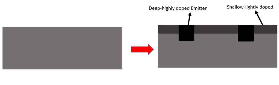
It all began with Mahammad Attala in Bell laboratories trying to overcome the bottlenecks of BJTs. Namely the higher power dissipation due to base current and hence low packing density, making it impossible to build advanced circuit smaller in size.
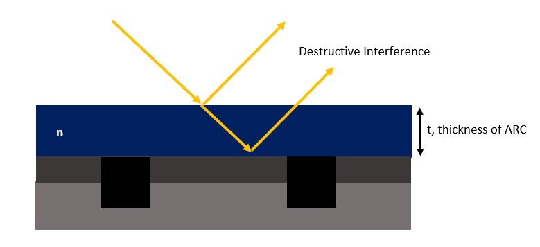
MOSFET Physical Construction
Now as engineers we have to be careful in understanding device details as a complete understanding would require backing-up with quantum physics explanations and at least 10 years of dedicated focused study. The key is to carefully listen to physicist and simply ask only for the details which are of our interest.
As far as device is considered, as engineers we need to know is answers to hows and whats only, but strictly no whys.
WHAT is a MOSFET?
Image Courtesy Wikipedia
MOSFET is a four-terminal semiconductor device, in which the resistance between two of the terminals is determined by the magnitude of the voltage applied at the remaining two terminals. The range of variation in resistance between two interchangeable terminals called source and drain is very large, extending from few milliohms to 100s of megaohms on relatively small voltage changes at the two terminals called gate and the base (or substrate). For simplicity manufactures internally short the source and the base, it thus becomes a three-terminal device and thus a voltage across gate and source changes the resistance between the source and the drain. This is not all to it, the variation of resistance is not simply linear, it is somewhat weirder, involving several twist and drama of semiconductor physics.
The gate terminal is metal plate separated from the body by an intermediate dielectric layer, SiO2.
The source and drain are two oppositely doped regions as compared to the parent base body of MOSFET.
HOW does it work?
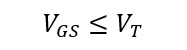
At zero source (or base) to gate voltage, the source and drain terminals are essentially open-circuited, as two p-n junctions appears between them in reverse.
For an n-channel type MOSFET:
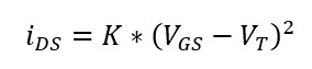
As we begin increasing the gate voltage (positive wrt source/base), positive charges begin to accumulate on the metal gate. The corresponding electric field is allowed to penetrate through the intermediate dielectric into the p-type base region between the source and the drain terminal. The exact distribution of field is however currently is beyond our strengths to explain. But the effect is quite intuitive that the minority carrier in p-type will start getting accumulating just below the gate. Not knowing the exact physics but at certain magnitude of voltage level, the devices develop a region so full of electrons that it acts as n-type doped region, and so is called n-channel. This particular voltage is called threshold voltage. The appearance of n-channel effectively results as if the source and drain were connected by a resistance. This 3- D channel’s length and width are inherently fixed by device construction however the depth is determined by the voltage magnitude. The depth is proportional to the excess of the gate voltage above the threshold voltage. This channel indeed truly acts as a resistor, if separation is more the resistance is more (r proportional to length), if the width is more resistance is less (r inversely proportional to the area), and similarly the depth dependence.
Current still won’t flow between the source and drain. If we now also begin increasing the drain voltage wrt source, the ammeter needle comes alive. So common sense says if we go on increasing the DS voltage the current will go increasing linearly, as the channel is an epitome of resistance😂😂😂, but not. The channel depth is proportional to the excess voltage Vgs – Vt. As we go on increasing the drain voltage this excess of voltage mainly responsible for the depth of the channel, constant at the gate end but begins to drop at the drain end. At a certain point, the channel shuts off at the drain end. It is obvious to suspect that current should drop to zero, but instead the current saturates to some constant value, and the phenomenon is catalogued in literature as pinching-off, and device is said to gone in saturation mode.
What are the operating characteristics and relevant equations?
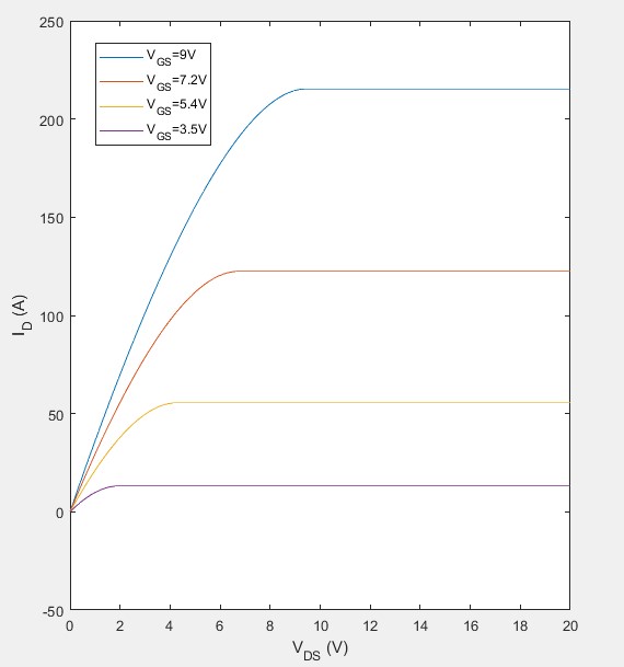
We study the MOSFET characteristics for different values of gate voltage. Until the Vgs is less than Vt the drain current remains zero for all Vds, as if open-circuited. For some Vgs greater than the threshold voltage, we plot Ids vs Vds. At much smaller values of Vds the current increases almost linearly, then due to narrowing of channel at drain end due to increasing Vds, the current saturates to a value at the pinch-off point.
Image Courtesy MATLAB
For all:
The drain-source is open-circuit:For all:
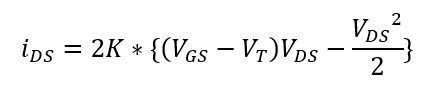
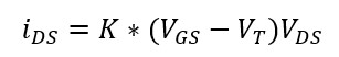
The source-drain current is given by:For small Vds, the square term can be neglected and response is approximately linear:
For all Vds ≥ Vgs – Vt, the current saturates at a fixed value, given by substituting Vds = Vgs – Vt:
“What is the distribution of electric field, why at pitching-off it still conducts current, derive the expressions”. All these are extremely interesting questions to take up, but as far as engineering is concerned it won’t help design the circuit any better, so we don’t mind answering them in free time.
The most repeating circuit pattern of our Electrical lives, we can’t trace anything down to something more fundamental than this. Right here we saw for the first time the gate and the amplifier. Let this pattern dissolve in our blood, imprinted in our DNA, memorized in our brains and printed on walls of our heart. Well, that’s how fundamental it is. 😂😂😂
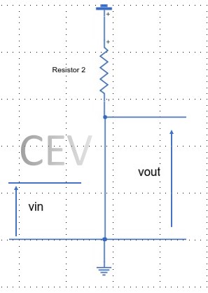
Before directly jumping to equations, let us first build intuition of how this circuit will respond to different applied input, which will allow us to flow through equations smoothly and swiftly.
So, what we need to imagine is the response of the circuit for different applied inputs.
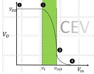
For some applied value of drain voltage Vdd, we begin increasing the gate voltage slowly. As expected, until it reaches the threshold point, drain and source remains open circuited. Current through drain resistor is zero and hence output voltage equals Vdd.
As the threshold potential is reached, the device just develops the so-called n-channel. Notice the current will just begin to flow and DS voltage will thus start dropping. Since the excess voltage is still smaller, and the DS voltage is sufficiently large to drive the MOSFET into the saturation region.
If we still increase the gate voltage then excess gate voltage would be too much for the DS voltage to keep the MOSFET in saturation region. With increasing excess voltage, the channels widen, dropping the resistance, increasing the drain to source current and thus dropping the drain to source voltage, and at one point DS voltage is lower than Vgs – Vt and the MOSFET enters the linear region. (often called triode region)
Notice we understood the operating characteristics is reverse order. To visualize in terms of how the MOSFET operating point moves on the operating characteristics will give more better idea.
At 2, the device just turns on and large value of Vdd immediately drives the MOSFET into saturation up to 3 where the MOS starts entering the triode region. Large dropping the DS, thus the output voltage to a very small value.
Mathematically:
Applying KVL, we have:
For region 1 to 2:
So,
Hence,
2. For region 2 to 3:
Current saturates at:
Thus, we have:
Parabolic drop confirmed.
3. For region 3 to 4:
Current should be given by equation:
Thus, we have:A rather useless relation. 😀😀😀
MOSFETs as GATES:
We know that any kind of combinational logic can be implemented using three fundamental gates namely NOR, NAND and NOR. How to use this circuit for a NOT operation is quite evident from the transfer curve itself.
For small input voltage range, the output lies in range of some high voltage level, representing digital high logic.
For a range of high input voltage range, the output drops down to a range of small voltage levels, representing a digital low. So, all we need to do is to set Vdd and strictly define the input and voltage range for low and high logic., and we are done, we have got an inverter (NOT).
MOSFETS as Amplifiers
We have seen the requirement of a man-made device called amplifier to obtain a crucial signal manipulation, called signal amplification.
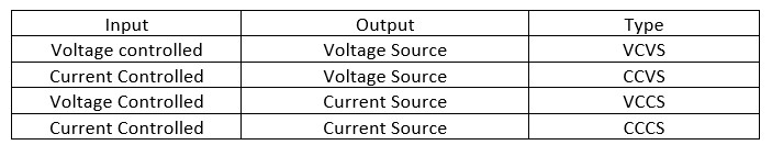
Amplifier in most general way could be called a source of energy which can be controlled by some input. Anyways there may be many more ways to look at amplifier, for example the earlier description of a transfer function block. More specifically this fits better into what we can call a dependent source. Before we understand what is amplifier let us understand what is not an amplifier. So, the element to be first excluded is a potential transformer. Though we can have a voltage amplification (step-up) we also have the currents transformation in inverse proportion so that power remains constant, similarly current transformer, a resistor divider, a boost configuration, etc. in which we have no power gain couldn’t be called amplifier. On the other hand, a MOSFET or a BJT appropriately biased, an op-amps, differential amps, instrumentation amps all are collectively called amplifier. Because we have a power gain at the output port wrt to an input port.
With one port as output and one input and third of course power port, theoretically speaking we can have at max 4 combination. Namely, we can have a current or voltage source at output, and we could have voltage or current control at input.
Any device for purpose of amplification invented in past or been invented or to be invented in future will fall in any one category.
The two-port theory becomes of immense utility, to easily describe different amplifiers in different matrix form, like Z-parameter, Y-parameter, h-parameter and g-parameter. We are constrained to not describe the theory in full detail; however, we will be building insight and motivation to study them.
We will use the same trademark configuration to do the amplification too. Isn’t this ground breaking? We had already built fundamental block for digital systems, and now we will again be using the same circuit for amplification which is of course an analog block.
So here it is:
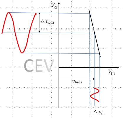
Remember, we didn’t talk about the region between 2 -3 when we studied this circuit acting as an inverter. We strictly worked in 1-2 or 3-4 region only.
The transfer functions in 2-3 region as previously computed is:
Though output voltage is proportional to input voltage, but nowhere close to linear. Remember what we have and compare it with what we wanted:
And here is the greatest revelation as the legends in this field had described for decades.
“The input signal is constrained such that the circuit approximately gives a linear response.”
And the revolutionary constraints are:
Giving a DC level shift, to drive the MOSFET in the saturation region, popularly called biasing voltage, and
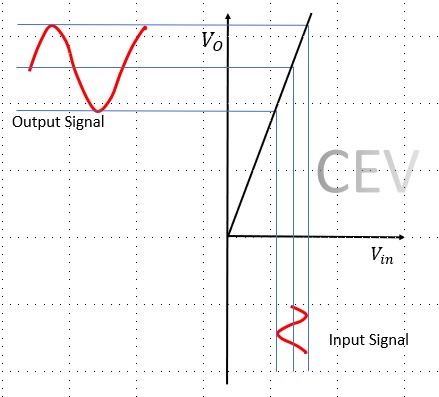
if the input signal is small enough the transfer curve is much close to a negative sloped straight line, which is in fact linear amplification.
If we zoom enough, here is how the amplification would look like. Notice inversion is there but a good linear amplification is also achieved.
We can also show that using the equation below that for small changes in input voltage indeed cause a linear change in the output voltage.
For,
We have,
So, we now comprehend the design problem of the amplifier as selection and operation at biasing point to get the best possible linear amplification for a given gain requirement.
And that’s a wrap. From here on we go on learning cascading amplifiers as one unit is not always enough to give desirable gain, which leads us to study the effects of stray and coupling capacitance which becomes especially troublesome when dealing with high-frequency signals, which then leads us to something called differential amplifiers, operational amplifiers, and as already describe we eventually take off from here.
All of this would be no so much use unless we also consider the energy consumption. Why it becomes so important can be understood by walking through some numbers.
Consider an inverter gate is build using the exactly as we have described.
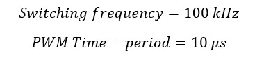
For SMD MOSFETs of today’s technology, typically
K is 1 mA/V^2, Vt =1 V, Vdd we take 5 V (TTL Logic), and let low logic at the output is defined between 0-0.2 V
When gate is OFF, high level at input and low level at output:
Power consumed by circuit is:
For order of 10 million of them:
This very rough approximation of power consumption is not at all pleasant to see for 10 million inverters in days when processors are reaching the range of 4-5 Billion of them.
We would require a dedicated diesel-generator set for one 200-gm machine. Of course, we do something about it, that’s why our laptops could be powered by a 60 W Lithium battery. The solution is quite a creative one. They call it CMOS (Complementary MOS).
In order to have incredibly high resistance, when the gate is off and very small resistance when the gate is on, a PMOS is used to replace the resistor. PMOS transistor has exactly the same operation as NMOS, except it is open-circuited for the high level at input and short-circuited at a low level at the input. Also, Vdd has managed to reduce to 3.3 V to reduce power consumption.
We didn’t learn all of the stuffs by sitting down and just glaring at MOSFETs. The entire credit for vivid imagination and connecting the dots goes to numerous books, all the lecture series, few research papers, beloved Wikipedia and all the awesome discussions we had with our friends.
We are thankful to a Lecture Series on Fundamentals of Digital and Analog Electronics, 6.002 MIT OCW by Prof Anant Aggarwal, two 40 lectures series by NPTEL on Analog Electronics by Prof Radhakrishnan, an introductory lecture series on Semiconductor Physics and Devices by Prof D Das IISc B, Basic Electronics Course by Prof Behzad Razavi of Princeton University. This article is result of rigorous brainstorming of ideas, concepts and insights gained from all the above-mentioned sources and then making our own speculations.
We are in the middle of a crisis. Not just the Covid-19, but the psychological turmoil of making money from every single dime available, even if it costs the whole economy’s meltdown. Does the short term or long term recession teach a lesson and put an end to this? It doesn’t seem so.
Something similar happened in mid-2008, whose foundations were laid in America’s housing market and the whole world had to face the consequences.
We’ll go step by step, starting from understanding the housing system and how it all collapsed. Don’t get muddled by the terms used ahead, as the concepts behind those are simple. The wall street people use these terms to keep the common people out of their way.
The Housing System
You must be familiar with the term mortgage. In case you are not, visualize it like this- you want to buy a $100,000 house, but you have only $30,000 with you. You approach a bank and ask for a loan. You pay $30,000 as a down payment, the bank lends you the rest of the money and based on your net worth, income statement, etc. bank decides a term of repayment and a reasonable rate of interest. Let’s assume this rate to be 10%. The bank allows you to pay it off in 30 years as monthly installments.
The house here represents a mortgage. Every month as you pay off the mortgage, you own the house a bit more and the bank owns a bit less. That’s how you own the house entirely after 30 years, and it’s no more a mortgage. And as the housing and real estate market is always soaring, real estate prices will always rise, as assumed before the crisis.
So your wealth will still be increasing even though you have to pay interest on the mortgage to the bank. It’s a win-win situation for all.
Building The Castles Of Money
Banks don’t always keep these mortgage bonds to themselves. They sell it to big investment banks and earn a nice commission. So the interests that you were paying on your loan went to their pockets now. But these small transactions didn’t keep the adrenaline of the big banks and investors running. So they came up with the idea of Securitization Food Chain. The idea was to bundle thousands of these mortgages on home loans along with mortgages on several other loans and sell it all together. This way, the yields will go up, and they assumed the risk to be still low as the housing market was always considered vital. They called it Mortgage-Backed Securities (MBS). The deal sounded like music to the ears of investors. So the investors all over the world leveraged lumps of money and invested heavily in these MBS, packed in a small magical box: a CDO.
A CollateralizedDebt Obligation or a CDO classified the above- mentioned mortgage bonds as per their risk of returns, the risk of trusting people that they will pay their mortgage on time. The ones who have a nice flow of income have a low risk and are rated AAA. Below them are AA, BBB, and the worst are BB-rated. BB refers to the houses owned by highly irresponsible people who hardly deserve to get a loan. These BB-rated mortgages are referred to as Sub-prime Mortgages. All these ratings are given by separate rating agencies that played a significant part in setting the crisis’s blueprint.All these bonds are then further sold to investors at a nice profit. The whole system was great because almost everyone earned a good profit and kept their cashflow running until things took an ugly turn.
The Inflation Of Real Estate Bubble
As the investors were earning good returns and demanded more MBS to invest in, but they couldn’t find any because most of the ‘eligible’ families already had a mortgage. So the banks started giving out homes to less responsible families, with zero down payment, no income certificate, nothing but just a formality of paperwork, and a promise of payback. They didn’t think of it as an issue because even if the families don’t pay, investors will own the house, which is also a great asset until there are so many houses for sale in the market.
In that situation, the ratings of those risky mortgage bonds would have gone down, right? But that didn’t happen. There was no one to ask the rating agencies how they were giving out the ratings. They were an authority in themselves whose ultimate aim was to impress their clients and earn money. The investment banks paid these rating agencies to rate their bonds and these agencies had no liability if their ratings proved wrong. They claimed the CDOs made by them had 90%+ AAA-rated bonds, but under the hood, it consisted of highly irresponsible homeowners who didn’t even deserve to get a $100 loan. So all these pieces of worthless junk bonds were bundled and sold as if they were gold, and no one bothered to look what’s inside. Investment banks were making profits by selling CDOs and agencies were getting paid for giving AAA ratings. Real estate prices skyrocketed as it was so easy to own one. A boom like this is called a Market Bubble– where everyone is so flattered with something in the market that they believe its demand will never go down and its value keeps on rising, even much more than its actual self-worth. But these prices are not more than an illusion created by fraudulent systems. These bubbles eventually burst and make a hard impact on everyone’s life. This time it was the Real Estate bubble in America that burst aloud in 2008.
Getting Insurance To The Crisis
The highly unregulated derivatives market of the USA allowed the bankers to gamble on anything. They could bet on the rise and fall of oil prices, bankruptcy of a company, or even the weather. Some of the psychopaths saw that the fall of the real estate was coming. So they introduced the Credit Default Swaps which were like insurance to the mortgage bonds. The buyer of these swaps will pay monthly premiums to the seller and the latter will pay colossal money to the former if the underlying mortgage bond defaults or fails. The demand for these swaps kept growing as more and more people realized that the housing market would crash. These swaps were packed in Synthetic CDOs.
So who was buying these swaps? The ones who were selling the underlying bonds. The investment banks were selling AAA-rated bonds in the markets and on the other hand, purchasing swaps on BB and BBB-rated bonds, as they knew the bonds would eventually fail.
Some highly corrupt officials even represented banks in the morning and the rating agencies in the evening. They packed the extremely risky bonds in the morning for the availability of bonds in the market and rated them 90% AAA in the evening for the investors’ sake. They also introduced a new complex derivative- a CDO of a CDO, called CDO Squared. The sole purpose behind their existence was to introduce more financial instruments in the markets, so there is always something to bet on. Let us see how they turned the whole world into a giant casino-
Suppose A and B are playing a game
C and D take a $100 bet on whom among A and B will win
E and F take a $1000 bet on whom among C and D will win
G and H bet on E and F
…. …. …. ….
There existed CDOs and synthetic CDOs as a bet against CDOs. Eventually, a $50 million investment had more than a billion dollars betting against it. The market for insuring bonds grew 20 times larger than the actual mortgage. The major players in this whole circus were investment banks like Goldmann Sachs, Morgan Stanley, Bear Stearns and Lehman Brothers, financial conglomerates like JP Morgan and Citigroup, securities insurance companies AIG, rating agencies like Moody’s, Standard & Poor’s, and many more. But from where was all this money coming? And how did they get the gigantic guts to borrow and invest? It was all possible because of the highly unregulated markets and the availability of cheap credit. Probably they all knew about the dangers they were playing with, but they also knew one more thing- they had grown so large that the government would have to save them if they go bankrupt, otherwise the economy would collapse. And that’s exactly what happened. The American taxpayer had to pay for all of their gamblings in the form of emergency guarantees and bailouts by the Federal Reserve. Several papers were published, a lot of people doubted about the crash, but nobody did anything tangible, not even the Federal Reserve.
You can now see how a system of billions and billions of dollars depended on a lie. Everyone was playing with a time bomb. This real estate bubble was about to burst and the whole world was about to hear it loud.
The Burst of The Bubble
When markets hit a little low in late 2007, people started to default on their mortgage and started leaving the houses. The number of these faulty people skyrocketed. The supply of houses in the market became much higher than demand, resulting in the breakdown of the prices. Now there was no sense in paying a $100,000 mortgage for the house worth only $90,000, even for those who were able to pay it.
Even well-off families started leaving their homes after taking their share, leaving the banking investors, small investors and lenders with a bunch of worthless properties. There was no more selling and buying of real estate in the market now as everyone knew it was useless. As every sector of the economy is deeply interconnected, the whole economy froze.
Companies like Lehman Brothers started filing for bankruptcy. Bear Stearns went out of cash. The stock market was on a bear run. The people had not seen the stock market steep so low in decades. People were thrown out of their offices in the peak hours of the day as their companies were no longer able to pay them. The so-called stock market experts were roaming on streets with their box of office essentials, which was now worthless.
The vast floors of Morgan Stanley and Goldmann Sachs, which used to trade billions of dollars a day, were now empty. The United States was no longer able to trade with other countries and the whole globe went into a recession that was never seen or expected in decades.
Five trillion dollars from the economy disappeared.
Eight million lost their jobs.
Six million lost homes.
And that was just in The USA.
Conclusion
In the post-crisis world, the government and the Fed should have taken responsibility for all the chaos and sent the gold plated corrupt bankers to jail. But nothing like this remotely happened. Instead, the so-called intellectuals blamed the small business people, laborers and employees as they always do.
The Fed and treasury department of The USA are still governed by the ones who were the crisis architects. The system never improved and the same things went on, only a bit modified to show everyone that they have changed.
Many major businesses in the globalized world are still void and it’s a bitter truth because that’s how the modern economies work. We may never know how many bubbles the global economy is having and how many of them have burst by the Covid-19 Crisis. We need to be aware of the lies in the market to keep our mind and soul together in times of these crises.
India has the 3rd largest startup ecosystem in the world; with a steady year-over-year (YoY) growth of 8-10%. Home to 55,000 startups, 34 unicorns, and 52 promising startups with a potential to become unicorns by 2022. India is a bustling land for startups and entrepreneurs with cut-throat competition at every stage. According to a Nasscom and Zinnov report, over 1,600 tech start-ups were registered in 2020, making it the highest ever added in a single calendar year.
With such hovering contention, you need to have an extra edge over your counterparts to succeed and to make it big in the current business scenario. So, with this notion, we CEVians, had a debate session on the topic — “Is an MBA necessary to be successful in business?”
MINUTES
In favour of the idea:
An MBA program covers a range of concentrations or specialisations that allow students to acquire the fundamentals as well as expertise in a specific aspect of a business, such as finance, marketing.
You get to meet and interact with like-minded people; which is an opportunity to build a powerful network and connections.
This degree is not just theory, the curriculum involves various case-studies of real-life business scenarios.
It’s easier to gain relevant working experience for a person with an MBA because it is considered a valid credential among recruiters. While for a person without an MBA, it is a tougher task.
Investors are more likely to invest in a firm if it has a person with credentials and experience. In case of lack of proven experience, having an MBA degree can bring better reliability for the firm.
After setting up the business, people with an MBA can plan the future strategic plans for stabilization and further expansion of the company.
Against the idea:
An academic degree doesn’t guarantee knowledge; practical experience is more valuable.
MBAs are expensive; better to invest that capital in your business idea.
In today’s world, you can easily learn about the necessary concepts through readily available learning resources on the internet and MOOCs.
For professional networking and work-related opportunities, there are various business-focused social platforms like LinkedIn, AngelList, where you can easily connect with an investor or a recruiter.
An MBA will only help you manage risks or avoid unnecessary risks, but setting up a business from the ground is a completely different story which they cannot ‘teach’ in business schools.
MBAs were originally designed to meet the demands of ‘administering’ the business in the early 20th century. Since then, the specifics of customers and the business environment have completely changed.
CONCLUSION
A professional degree like an MBA can certainly help you in understanding businesses better; it is not mandatory. Nothing can guarantee success in your business. According to a report, out of every 5 business leaders, 2 do not have an MBA or a postgraduate qualification. This further ascertains the fact that pursuing an MBA or not, is explicitly a matter of choice.
Majority of wealth in the world is with the minority of people leading to unequal distribution of money and issues such as poverty in society. As a solution to this problem, what if all the wealth in the world is divided equally among the people so that no one is poor and no one is rich. Sounds like an awesome and innovative idea, right??
First of all, the idea of equal wealth among the people will end competition. Competition is the force which thrives innovation, the development of new ideas, new products, services, and thereby development of economy and society. Competition improves the intellect of an individual and a whole society . The hunger for betterment and wealth creation; to be the best in class is what improves systems and makes any society futuristic. For an analogy, let’s assume a class of students. For this particular class, it is decided that whatever marks the students will get, it will be averaged and equal marks will be given to each student. In this scheme, the capable students will not put extra efforts, study and learn as they know this will not come to them in a whole whereas the incapable will become idle & lazy thinking that the others are doing their job for him & that he need not do anything . This will lead to deterioration of one’s intellect, lack of knowledge and skills.
In such a system, ingredients essential for development of an individual and a society such as ambition, hard work, dedication, excellence, ethics, etc. will not exist. An industrialist and a beggar have a huge difference in the mindset. An industrialist will invest the excess money in various industrial sectors and workforce giving employment to people whereas a beggar will simply spend the excess money relentlessly. If all the people have the same purchasing power, this will lead to inflation for a few ranges of products and others will lose their value and importance in the market. This will have a very bad effect on the cash flow in the markets. For maintaining global peace one of the essential factors is monetary power so that people can be led in some direction. The concept of equal wealth among all destroys this power.
The above ideology of equal wealth among all will require an enforcing organisation for its implementation in the long run. This is because it is impossible to make every person walk on the same principle; the monk principle (give free service to the society and to be satisfied with what one has).
Implementing the above ideology will decrease the value of money, deteriorate lifestyle and will lead from social equilibrium to a worldwide chaos. Hence, this ideology of a chaotic state is not applicable to the real world.
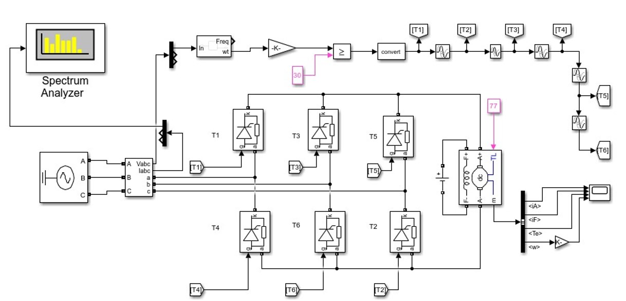
Our final aim in one sentence is “to make safe electrical power available to all 24*7 round the year, round the decade and so on”.
And that phrase says almost everything we require to do.
As an electrical engineer that’s all what we want to do in our life, everything for it. From now on, anything we think or do professionally is going to manifest this final aim, have you ever come across anything holier than this.
We have very carefully phrased the paragraph to capture whole of electrical engineering in its entirety.
So it goes….
“Safe electrical power”: indicates the first necessity i.e. the safety of electrical power, which is all about operating the power system in a strict pre-defined range of parameters including active and reactive power levels, voltage, current, power factor, and distortions.
“Available to all”: indicates the affordability and treating electricity as not just mere commercial commodity rather a basic service for all. The economy of the power system is essentially a science of figuring out how much to turn the knob of which power plant.
“24*7 round the year”: set for us the reliability feature of the power system. Now, this includes very smartly designed protection systems which largely sits idle just waiting for the time to be called in.
“Decade and so on”: indicates the security feature of the power system that we wish to keep on powering the world as long as human exist which requires to keep looking up for new sources of energy. Notice we may be interested in anything that can jiggle the electrons in the wire at 50 Hz. So solar, wind, geothermal, tidal, and even Nuclear Fusion and Fusion are all the cards we keep stocking in our free times and weekends.
Any subject you will ever study have its application in at least any one of the above-mentioned categories. Just fast-forward how the subject will help in achieving this final aim and you will get hugely motivated and interested to take it.
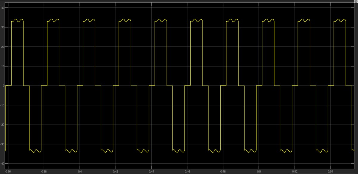
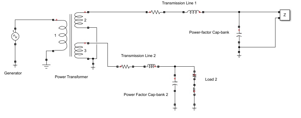
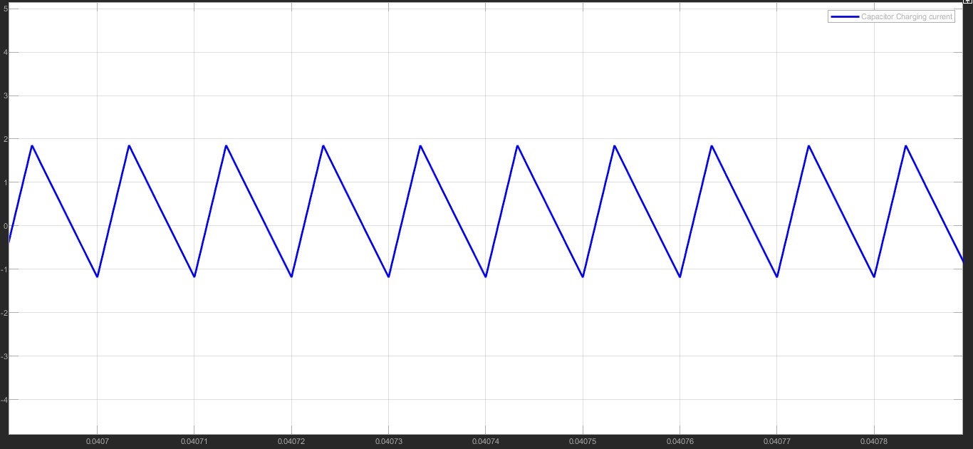
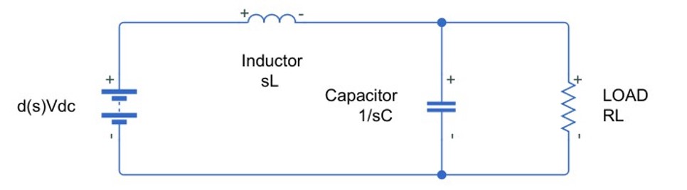
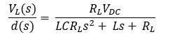
Another facet we miss is enabling ourselves with the tools of engineering. And one of them is Simulation Software. The simulation software has immense capability to add to the fire and gives wings to our imagination. No doubt anything that you could ever do with simulation software could also be done by your hand on a white sheet. But the sheer advantage of vivid visualization of things, accuracy and validation of results and ease with which things could be done is truly great. On your desktop you can build anything you want a large power system to visualize the load flow and system natural frequency (as we did in Harmonic Resonance Study and fault analysis) using MATLAB, a microcontroller-based system to do crazy things (as we did in Harmonic Analyzer) using Proteus, an analog circuit comprising of the wonderful op-amps to perform any mathematical functions (as we did in power module) using MATLAB, you can plot with extreme accuracy and detail and easiness the response of any transfer function using bode-plots, pole-zero plots, Nyquist plot, (as we did in designing buck converter) using Scilab You can tweak and play with the drive system of any machine like PMSM, BLDC, Induction motor, DC motor, etc.
One of the crucial practices in engineering is a sound appreciation of comparison between all ranges of systems and equipment.
Various systems types (machines, circuit configurations, etc.) are available at our disposal, what enables us to make a good engineering decision to go with a particular type and not with another for a given specific application is our ability to distinguish between all options available.
Will you use a DC machine, a Squirrel Cage Induction Machine, or a Synchronous Motor?
Will you use a Cylindrical Rotor or a Salient Pole Rotor Synchronous generator?
Will you use a Ward Leonard Drive or a Static Ward Leonard Drive?
Will you use an HVDC line or an EHV-AC line?
Will you use a Voltage Source Inverter Drive or a Cycloconverter Drive for V/F control?
Will you use a Synchronous Condenser or a Static VAR Compensator?
Will you use a MOSFET or an IGBT?
Will you use an Overcurrent Scheme or a Differential Scheme for transformer protection?
It will take another 5000 words to carefully analyze which choices to make under which conditions, so we will leave on your own to figure out why!
Sooner or later we will be confronted by all these sort of real-life MCQs in our career, to make a good, economic and futuristic decision one has to be very critical minded while studying and comparing all varieties of systems among systems.
Another thing we want to bring to your attention is having a mindset to pay attention to all the electrical engineering stuffs going around you. Like noticing the voltage and power levels of various equipment and systems (traction operating at single phase 25 KV, wattage ratings of household items), noticing design and structural details (the reason behind the shape of a three-pin plug), visualizing and analyzing waveforms and distribution of fields in 3D space of the street power lines, even noting which brand of EV uses which types of machines and so on. This helps in either answering a wide range of short questions asked throughout and more importantly helps understand and connect better while actually studying those things.
Having a technical discussion with a loving friend can immensely help in getting oneself easy and clear with the terms and concepts which are otherwise sound so technical. It is a very effective way to sharpen one’s engineering language accent of talking and thinking. So, we are not just engineers on our working table, in our classes and in our labs, to unleash the full potential we need to be literally obsessed with these stuffs in all spheres of our lives from personal to public!
Since we have so much stressed upon enabling nature of these tools learnt in four-year course, we must now lay down its disabling feature.
And lets us illustrate this with a small regular classroom incident:
In our second-year lecture, Prof. AKP Sir asked us to differentiate between the underground system and the OHT system, each of us made him count every technical detail like less corona loss, lightning protection, fault location, etc., very technically. But all of us missed the most critical point for which some great engineer had devised the underground system for, we failed to see that the OHT occupies more physical space than the underground system. That was the evidence that our natural intellect was hijacked by the professional knowledge.
We had acquired the technical knowledge in the wrong motive. We think that it is the most crucial tool to enable us to see different and otherwise difficult things, whereas the truth is that it is just an aid to our natural thinking to understand and describe the things easily. We are so trained to think in a loop that we literally miss very crucial points which if we were not trained could have thought about.
So, it is very important to be always grounded in terms of thinking and not take many facts for granted.
In the end, we have:
Image Courtesy: Goalcast
Conclusion
Engineering in the 21st century has become quite well defined, we now have sophisticated understanding of things, unlike in the past when people considered magnetism and electricity different. Now problems have become accurate in their own terms, there are much fewer compelling questions of “why” rather than “how”. For example, how to accommodate renewables on the grid, how to solve the battery problem, how to spin motor greener and smarter, etc. Throughout the course we are presented with all the necessary tools and hacks which are very logical and easy to understand with little mind-force.
On the other hand, in our everyday life due to some reasons we take up the wrong fight. We are busy somehow dogging the assignments and the quizzes and so on, completely missing the true fight we actually are in, and that makes a difference between enjoyment and getting oneself literally tortured.
NOTE: All the statement made in this blog are authors own mere speculations it may be wrong, so an active reading is greatly expected. Don’t’ keep the statements until you yourself get sure of validity.
The military world has a striking work culture, in fact there are many, and today we are here to reflect on one particular culture of our interest. When a group of soldiers come from any dangerously tiring mission, they don’t drop their weapons and just fall to their beds, as we folks do after our classes and labs. They wash their wounds and immediately sit down to catalogue with utmost honesty an account of what happened in the battle-ground. They critically examine what went well and what went wrong. The leader then reaches to high commands to give a debrief of the operation.
Well, this has a very precise purpose; it aims to carefully learn and bring lessons to their fellow generations of young soldiers which otherwise could unleash catastrophic fates.
They keep on updating the never-ending list of how to not get killed in a fierce encounter with the most inhuman truth of humans.
If we could bring a minute fraction of how things are done in the military, we can have profound changes in our everyday conditions deep inside our national boundaries. On the same line, we are here to note down with similar honesty a journey of four years which we popularly call engineering.
With the same vision to give an account of what all went well and what went utterly wrong.
Electrical Engineering is a 200 years old science having Michael Faraday and JC Maxwell as forefathers followed by the genuineness of Nikola Tesla, T.A Edison, Steinmetz, CL Fortescue, Harold Black, M Atalla and a long legacy of great exploring minds. The course condenses important and most relevant works in just four years, which is in fact small as compared to two centuries, but still not a cup of tea.
Four years is quite a large time to hang-on, thus many times people lose the bearing of what they are into, unable to situate themselves with ongoings and hence lose their sight.
By the end of this piece, you would be presented with a panoramic view of the scene you hopefully be confronted-with after your own four years, so that you can always reflect and find yourself.
In the beginning, you may be very interested in learning how the whole energy system works and the hard truth is you will never get to know about it in the first year itself, in fact even the slightest gist is rare. You have to go through many building theories, sometimes grudging math, few “boring appearing” experiments, etc. to finally be able to appreciate the whole picture. You will come across Fourier series, Solutions of differential equations, Complex Algebra, Symmetrical Components, Laplace and Perks Transformation, Tylor expansion, some dead appearing theorems like superposition, Thevenin, etc., behavior of electric, magnetic forces and electromagnetic phenomenon, a mesh of transistors and MOSFET called operational amplifiers, which at first sight will hardly make sense for great application in power systems. But when you develop your arsenal consisting of all these simple but powerful theories, tools and gadgets, later you literally get amazed by their capacities.
You have the Eureka moment in final year!
The significance of Fourier analysis to understand and analyze behavior of wide range of non-linear systems (like inverters, rectifiers, etc) and applications in the study of power harmonics, the solution of differential equation to figure out the transient behavior of almost all the electrical subsystems from machines to faults in transmission lines to the study of the opening of the circuit breaker, the use of complex algebra to facilitate AC calculations, the utility of symmetrical components to study unbalanced conditions in polyphase systems, the use of Laplace Transform to turn differential equation to simple algebra, the Tylor expansion to approximate trigonometric values using analog circuit, the use of Thevenin and superposition to enormously simplify network calculations, operational viability of electric and magnetic forces and electromagnetic phenomenon to executes all range of machines, measurement instruments and relays, the op-amps to amazingly implement any desired mathematical operation and so on.
We goanna list the important theorems and prevailing concepts and their application in the larger scheme of things, we want to put in front of you a panoramic view of how it would look like after you get through this amazing four-year journey. We wish to put all the pieces together to help to get a grand view of the symphony of 21st-century power systems.
The Maxwell’s Laws
“The scope of these equations is remarkable, including as it does the fundamental operating principles of all large-scale electromagnetic devices such as motors, cyclotrons, electronic computers, television, and microwave radar.”
-Halliday and Resnick
Majority part of Electrical engineering is the manifestation of Maxwell’s laws. The KVL, KCL, the machine theory almost all of it can be understood by starting with four maxwell law or conversely start reasoning any stuff it will eventually boil down to Maxwell Equations.
Let us illustrate that the most basic laws the KVL and KCL are mere special case of the third and the fourth equation.
Consider a simple resistive circuit excited by a DC voltage source.
So here current would be:
Why?
Because: V= IR
Why?
Because: V-IR = 0 😂😂😂
Too much obvious, isn’t? Just be in game, it will show how facts which we take for too granted come to diss us someday.
Let us ask one more, “why?”.
So, answer is because the algebraic sum of voltage in a loop is zero.
Why?
Now you see our EE theories falling apart. Many of us would not be able to answer this “why”, because we take KVL for granted.
Let us put one example where KVL will just tear apart completely.
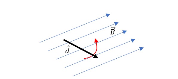
Assume, this coil now is in a magnetic field and is externally rotated at constant RPM, somehow maintain the contacts with battery.
Apply KVL now, V= IR should still hold, but we get horrified by what ammeter looks like, it shakes.
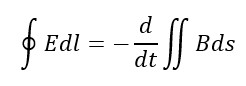
So, the catch is KVL is just a special case of some other law. That other law is the third law of Maxwell. It says line integral of the electric field around a loop is equal to the rate of change of surface integral of magnetic field with the loop.
Popularly quoted as “the EMF induced in coil is rate of change of flux through the coil”.
If the right-hand term is forced to zero, we get KVL.
So, whenever we apply KVL to any loop of a circuit we unknowingly set the rate of change of flux linking the circuit to zero, if that is not the case as above, we get wrong answers.
We know for sure that KCL is also a special case of Maxwell Equation, but we by now, are not quite able to manipulate the equations, it would be updated shortly.
You can also write to us.
The Grand Theory of Machines
Very broadly speaking, there exist two types of machines, the machines running on DC Supply and another on the AC Supply. Under the DC category, we have shunt, series, compounded motors, under AC category we have Induction horses, Cylindrical Synchronous and Salient Synchronous machines. Other machines like BLDC, Stepper, SRM are extension of these basic machines only. It takes over two semesters to get all of them in our heads, and that to just vaguely.
Nearly all the important calculations on DC Machines can be made by three simple equations.
All the engineering relevant parameter of an Induction Motors can be deduced by drawing the equivalent circuit.
This simple diagram all the details the rotor speed (if synchronous speed is known), the current, power factor, the core loss, the air-gap power, the rotor copper loss, the mechanical power and the torque.
For Synchronous Machine we usually draw phasors to get all-important numbers like Torque, power, current, power factor.
Dropping down all the details of how the machine works almost all numerical can be solved out if one remembers the equations, equivalent circuit and phasors as mentioned above.
But it becomes tricky when one tries to explain them, as for different machines we have to follow different approaches to explain the generation of forces and so on.
General approaches are:
The DC motors rotate as current wire experience a force in a magnetic field, Induction Motors runs by virtue of the principle of Electromagnetic Induction, and Synchronous motor runs as rotor field gets locked with the stator field.
We know you would have squeezed your eyebrows as you walked through this paragraph.
There may be several lines along which they may be unified, but here we present our own speculation to understand and explain the operation of all kinds of motors using one single theory.
Basically, the force generated in all the motors (DC or AC) is analogous to force experienced by a magnetic dipole in a magnetic field, trying to align along it. Theoretically, if the angular position in space is stationary or both moving but stationary to each other, then the torque will be constant.
Notice that for given magnitude of the vectors the forces depend on the angle between them, maximizing at 90-degrees.
In DC motors the field produced by stator is fixed in one direction, the rotor though rotating using the help of brushes maintain the current distribution at any angular position in space fixed, irrespective of which conductor coincide at that position it always carries same current in same direction, thus giving rise to another magnetic field (or we shall say dipole) which also remains fixed in space at 90-deg. It is these two dipoles which generate torque and make the rotor rotate.
Induction Machines doesn’t seem to work on this analogy in any way.
Well, let us check.
So, the stator produces a rotating magnetic field at a fixed synchronous speed, meanwhile, the rotor rotates at speed somewhat less than synchronous speed, depending upon the load on the shaft, or depending on slip “s” as we say. Speed of rotating magnetic field of rotor is sNs wrt to rotor structure, this structure is itself rotating with a speed Nr, so the speed of rotor field as seen by the stator field is sNs + Nr- Ns i.e. is luckily zero, hence again we can explain the torque on the rotor by the interaction of two moving magnetic vectors but fixed relatively.
In Synchronous Machines, it’s easily identifiable that field produced by the rotor is fixed wrt to rotor structure but rotates at synchronous speed wrt stator as rotor itself rotates mechanically at synchronous speed. The other field produced by a balanced stator is obviously rotating at synchronous speed, thus again allowing us to imagine torque on the rotor due to interaction of fixed magnetic field and a dipole.
That gives us the freedom to explain the working of all those machines in one shot-one go.
We are also trying this theory to get around Vector Control of Induction motor.
We haven’t figured out but we wonder if similar analogy could also be applied to BLDC, SRM and Stepper too!
Until now we were uniting all the machines to understand the rotating machines as a whole, now let’s divide them.
And when we try to divide them, basically we are entering a domain called Electrical Drives System, in which clear and very sharp boundaries are drawn to distinctly identify the machines for their purposeful use in a given required operation.
Almost all the major subjects of electrical engineering come under the umbrella of electrical drives. Obviously, the machines itself, power electronics for proper power conditioning, control systems for power electronics, the analog and digital electronics for control systems, and lastly the microprocessor for making those electronics alive.
The DC though provide easy speed control, but the problem of sparks and heavy maintenance makes them unfavourable.
The Induction Motor being a very simple, rugged, cheap device and sparkless operation makes them suitable for almost 75% industrial applications today. The bottleneck of Induction Machine is its inherent characteristics to draw reactive power from mains. At higher power levels power factor becomes a crucial parameter as it greatly affects the efficiency, motor heating, overall power system overloading, drop in supply lines, etc.
A higher power rating synchronous motor with god-like control over the power factor is an obvious choice. Not just UPF it can be made to operate at leading power factor, thus balancing the reactive power requirement of industrial setup as a whole.
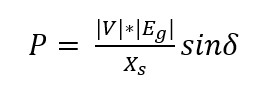
The Power Flow Equation
Consider a very generalized two-port network. Using KVL we can figure out the current and hence the active and reactive power flow at both sides.
The apparent power at receiving end:
As a power system subject always tends to neglect resistances, so the active power can be approximated to:
And the reactive power can be simplified by assuming δ small:
These two equations apply for transmission lines, synchronous motors and generators as well, and are very prominent equation in EE.
Assuming the bus to which synchronous generator is infinite bus, this real power equation becomes useful in the swing curve and is used to study the steady state and transient stability of the gens.
We will see how it is useful in transmission line.
This equation (1) indicates that the direction of power flow is determined by the delta angle (commonly called power angle) and it worth noting that the power flow can occur from to low voltage to high voltage level too, if delta allows.
The equation (2) indicates towards a very crucial phenomenon in transmission line. If the Reactive power is more than there will be more drop in voltage, and conversely more voltage sag indicates towards more reactive power being extracted. Transmission lines being a very high voltage system hence the Voltage Regulation of 5-8% is required, so a strict control of Q is desired.
Moreover, the reactive component of current would cause an unnecessary ohmic loss in long lines as well as underutilization of every component. Reactive power rather than being supplied from generating station it is good to provide it locally hence distribution station began switching their capacitor backs when such voltage sags occur.
Open-air substation capacitor bank
The Indispensable Control Theory
Control Theory is about dealing with disturbances which is the absolute nature of nature anyways.
If we had known for sure the response of any system for given input then achieving any desired output would haven’t been much difficult.
For example, if you know for sure person will slap you back if you slap him first, then it won’t be a difficult task to get oneself slapped. The catch is “surety is not there”, he might forgive if he is in a good mood you or even give you a headshot if annoyed, at worse.
Control theory largely accounts for the disturbance, how to still maintain the desired output even under any uncertain disturbances.
All the parameters on which we judge the system performance like fast settling time, less steady-state error can be easily achieved with a suitable controller in an open loop. Close loop, on the other hand, creates stability issues to most of the stable plants, brings the problem of sensor noise, but the greatest advantage is that it takes into account the disturbances (changes in plant models, or externals disturbances, etc.), which becomes of extreme interest in a natural environment.
Power System is a dynamic system, by that we mean it keeps on changing all the time. The tremendous amount of energy that is being generated should always be equal to the energy consumed at any instant because there is no storage in between. Thousands of generators are just only spun and excited to just exactly meet the load demand of millions of consumers spread over a vast geographical area.
This is a huge challenge if we think more deeply.
If we had known exactly the load demand (say 10 W) and we know the loss in lines (say 2 W) and generator losses (say 0.01 W) then we would have calculated the exact rate at which we should fire the coal and we are done and have gone out to play soccer.
Problem is that 10 W never settles. Every time we turn-on even a light bulb the power system adjusts itself to a new equilibrium state.
The pressing of a switch, falling of a tree on lines, or falling of electric poles itself etc. are all different types of disturbances and fixed safe level of parameters like voltages and frequency are desired output of the system, with input being the coal fire rate or diesel-burning rate, or watergate opening, etc. Without feedbacks, we can never do that. Though it’s not like there is just one feedback going back to power stations from the load centres, control system exists at all levels, and it leads to the overall system working as if it were a one close loop. Hence studying Control Systems and Theory becomes of extreme utility to us.
How would we do that will unravel the need to study Analog Electronics, Digital Electronics and Microprocessor and Microcontroller Systems carefully.
The Leverages of Power Electronics
One of the leading reasons why Edison lost to Nikola Tesla in the war of current was the inability to manipulate the DC unlike AC power whose voltage levels could be pushed to extremely high levels with easy by the use of transformers and thereby improving the efficiency and performance of whole power system, leading to the concept of centralization and utilizing the economy of scale.
DC systems like DC motors and DC transmission lines, were hence largely suppressed as the growth of AC accelerated, but they do have their own advantages. And now with hacks of power electronics, DC systems are now gaining ground as complementary to AC systems.
Let us illustrate by a few examples where AC systems have bottleneck and the power electronics comes for their rescue.
Case 1: Power flow in AC lines
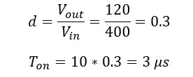
The limit on maximum power transfer through a line is the thermal limit and dielectric limit, if the system is already at ultra-high voltage levels then thermal limit becomes the ultimate limit.
So, what we can do to achieve the maximum transferable power.
Voltage levels are raised to dielectric failure, Delta we cannot increase beyond 30-degree. So, the only controllable parameter in our hands in line impedance.
To achieve that max limit decreasing the line impedance is only at our disposal, if there is no control over line impedance then the power lines will be greatly underutilized.
Power electronics allows us for a clean, simple stepless control of effective line impedance, called the series compensation.
Not only that PE now has matured enough to DC manoeuvrings at extraordinarily high voltage and current levels, which enables the concept like HVDC lines that has extremely desirable properties of easy power control.
The direction of power flow was dependent on delta angle, and there is not too much freedom in manipulating this angle nor it is easy it light of stability problems.
HVDC however doesn’t suffer from this issue.
Follow this ABB Hitachi Power Grid commercial advertisement on how the HVDC was only capable to do what they did.
Case 2: Speed Control Problem in Induction Motors
DC Motors were predicted to become obsolete by the end of 1960s but one can see them alive, in fact quite prosperously.
Why?
It has very desirable operating characteristics.
For shunts motors, if torque demand increases so armature current would be increased proportionally if the terminal voltage is kept fixed the change in current would not affect E much as small armature resistance diminishes the effect. Hence speed remains almost constant.
If we want a higher rotor speed, we just simply decrease the field flux.
If we want to operate in a lower speed range, we decrease the supply voltage.
Notice y appropriately changing the parameters many desired characteristics can e obtained.
However, for induction machines, one doesn’t have such a degree of freedom.
Ones a machine is designed its maximum slip gets fixed. Obviously, the maximum slip would be kept low for better efficiency. So its rotor RPM gets limited to a very narrow range. Beyond this limit, the machine would be unstable as we know.
So, we can get a great range of torque for almost constant speed. But varied speed operation is abandoned.
Power Electronics has helped overcome the speed control problems of Induction machines and synchronous machines with the advent of VFDs and other advanced scheme called vector control which almost transforms an Induction Machine to a DC Shunt Motor.
The Torque speed characteristic can be squeezed or expanded by varying the frequency and taking care of supply voltage as other saturation problems or insulation kicks in.
Only at the mercy of power electronics, those drives could be built.
And this list is getting larger and larger every day where power electronics somehow imparts the most favourable characteristics of DC systems to AC systems.
Well devices used in “Power Electronics” called power diodes, power transistors, power MOSFETS, IGBT, don’t differ from “Electronics” counterpart in terms of what they do, however, a simple diode has two layers p and n but power diode have three, so along with having power in front of their names power electronics devices vary greatly in construction.
To be continued………….
NOTE: All the statement made in this blog are authors own mere speculations it may be wrong, so an active reading is greatly expected. Don’t’ keep the statements until you yourself get sure of validity.
Reading Time: 12minutesOn the occasion of auspicious Diwali, team CEV wonders what could be more relevant and important other than to talk about harmonic resonance!!
Haha, but no kidding!
Since Diwali is a festival of “lights” and in these days harmonics are unanimously voted as the most popular villain in electrical world to turn the “lights” out!
Well if you have been a new reader at CEV, we would like to bring into your notice that our CEV’s Aantarak division have been literally obsessed with power harmonics for a long time now. We had carried out in-depth preliminary literature recon followed by collaborative effort to develop our own harmonic analyzer from scratch. Both can be accessed by following links respectively:
Continuing the same lines, we walked another mile to get ourselves around the harmonic resonance phenomenon, which otherwise has been tagged as seriously spurious.
We really hope to wind up our intuition for harmonics and related phenomenon in this last blog of the series, so we wish to describe it in its full glory. So, you might encounter some repeating themes, apologies for that.
The Crisp
For any domain, having a glance of history really helps in getting a larger picture of the things. Being aware of the historical background greatly aids in understanding the things with continuity and help in extrapolating the ongoings to get some future insights.
So EE folks haven’t begun struggling with harmonics in recent times, infact one can trace it back to early 20th century when power systems were in its earliest phase. Charles Proteus Steinmetz, yes the same engineer who taught the world how to draw the equivalent circuit diagram of induction motor and gave us a handy notation of “j” to simplify our AC calculations had made an excellent introductory paper in harmonics. At that time due to inferior core materials transformers and motors saturated, giving rise to these problems. However, now the problems- harmonics pose remain unchanged but the sources and impact have been magnified manifold.
21st-century power system seems to be literally littered with inky-dinky semiconductor devices which draws currents which are severely offbeat from sinusoidal nature, moreover, the advent of high power electronics has made the situation more vulnerable. Technically these devices/loads are called Non-linear devices/loads, and problem they pose are quite spurious in nature. We know that high-frequency components of these currents called harmonics interact with power system in ways leading to overheating of components, flickering, circuit breaker false trippings, or even causing catastrophic events like a wide-area power outage (aka. Blackouts), as reported by many utilities in recent times across the world.
These harmonics can tune the capacitor banks used for power factor improvement and voltage stability in resonance with the power system components and lead to blowing up of the banks and causing further contingencies, like voltage collapse, etc.
In this blog, a detailed analysis of power factor banks, non-linear loads, resonance phenomenon in RLC, and lastly the resonance in power system due to harmonics is carried out.
One more note, you might be aware of the MATLAB company tagline, it reads “accelerating the pace of science and engineering”, and CEV is really goanna help MATLAB do that here. We will use appropriate MATLAB simulation models to verify the theory and bring home to the readers a sophisticated understanding of the phenomenon.
The Skyrocketing hopes!!!
The flow
Power Factor Capacitor Banks
Thevenin’s Equivalent of Power System
Electrical Resonance in RLCs
Harmonic Resonance with PF Capacitor Banks
Harmonic Resonance, is among the most dreaded phenomenon the power system harmonics are observed to unroll.
ABB, the mega-giant in the power system industry tries to bring on the table the significance of eliminating power harmonics by its product commercial.
Though being regarded as the most suspected reason for unexplained failures of electric utilities the harmonic resonance is a phenomenon that could be explained in a paragraph of no more than 100 words only, you would be able to do it the small kids around you, by the end.
The story begins from the power factor capacitors banks……
You might have appreciated the fact that the use shunt capacitor banks across the electrical motors (lagging loads) can improve the power factor greatly.
The underlying idea is to provide the reactive power locally instead of drawing it from the system thereby reducing the supply current and preventing the elements of the whole power system (from T-lines down to the generators) from overloading.
This concept can be intuitively understood by use of following graphs.
Consider a sinusoidal voltage applied across an inductive load, result is a lagging current.
So, the convention is to simply connect a capacitor bank of required capacitance. Since the capacitor is in parallel so the voltage across it is in phase with load terminal voltage, and the current through it is obviously 90 degrees leading the voltage across it.
The phasor diagram:
The waveforms are like:
Adding the parallel currents to get the supply current:
So, it could be easily seen that the peak of the resultant current has been reduced, at the same time the power factor angle is also reduced hence power factor improved!!
This same result can be concluded by simply adding the current vectors mathematically.
So, what exactly is happening here?
The picture becomes crystal clearer if we try to simulate an RL load with shunt capacitor and visualize the instantaneous power consumed by each element.
By putting appropriate parameter values, it could be seen that when inductor is absorbing power the capacitor is releasing its stored power, and when the inductor is releasing the stored inductive power in its magnetic field, the capacitor is absorbing it in its electric field. It is this inductive and capacitive power, are collectively called reactive power, which just flows in the system but never manifests itself as real power, rather just oscillates. If this power exchange becomes equal then no net reactive power is drawn from the source.
So final result is “significantly reduced net reactive power drawn from the source and so is the supply current”.
Question: Do you think that the capacitor in ceiling fans of households serves the purpose of PF improvement?
Now to analyze the effect of shunt capacitor for non-linear loads, i.e. loads that produce harmonics, we have to follow a different approach, a completely different line of attack.
However, the theory we just saw is equally true, but as far as harmonics are concerned, we are more interested in first understanding the frequency response, rather than power calculation.
Some of the most basic and prevalent techniques used everywhere and all the time in power system analysis are first required to be grasped before we try to understand what happens for non-linear loads.
The concept of Thevenin’s equivalent;
The concept of current injecting vector
The concept of superposition
Thevenin’s Equivalent of Power System
Consider this point of view, the two-terminal is supplying a single-phase non-linear load, also conventionally a power capacitor is applied in parallel to supply reactive power locally. The black box here is an abstraction of all the distribution and transmission transformers, transmission lines and the generators and whatnot, all working in synchronism.
So, the Thevenin theorem says that the black box can be represented by an equivalent emf source and an equivalent impedance in series, called Thevenin’s voltage and Thevenin’s impedance respectively.
The Thevenin voltage is simply the open circuit terminal voltage.
And the Thevenin impedance is the impedance seen by the load given all the voltage and current sources are deactivated.
Once the Vth and Zth are known, to know the impact of connecting a load impedance to already loaded grid we don’t go on solving whole vast electric mesh again. A revolutionary French electrical engineer LC Thevenin in 1880s came up with a revolutionary method to enormously simplify the large electrical circuit.
Find Vth and Zth. Now turn off all the sources, connect the load wherever required, excite the point with the negative Vth, find the drop and add the drops algebraically to already existing system. This is applicable only for linear system by virtue of superposition theorem. This line of attack is chosen when the load impedance is center point (i.e. load impedance is known). This is quite a popular technique and is implied to calculate the impact of loading on different buses of system, fault analysis for a known value of fault impedance, etc.
Now, if impact of a given load current is point of attention (rather than the load impedance) then we use slightly different approach. We turn off the source and inject an equal load current at the point of connection of load, find drops at different nodes and again added algebraically to the existing system.
Now in this case of harmonic resonance study, notice we are utterly concerned with the load current. Our prime moto is to see the impact of a given non-sinusoidal load current on the system.
Here it is important to reflect to one important fact. Our power system is built up of thousands of different kinds of elements, the generators synchronous and asynchronous IMs, the transformers, T-lines, cables, a huge variety of loads, yet all of them can be modelled as a combination of just three fundamental elements, resistance, inductance and capacitance.
Q. How would you modify the Thevenin equivalent if the power systems have power electronic components?
So, it is all those little-tiny things learnt in early engineering classes of circuit theory comes back to manifest in harmonic resonance and other complicated higher phenomenon. Here we realise that solving the RLC circuit is not dull, unless we know how far-reaching are the meaning of those Rs, Ls and Cs in a practical applications.
But all of these theories are strictly applicable to a linear system.
Think for a second how to manipulate the tools for the non-linear currents.
So, lets revisit our aim, our aim is to find the impact of non-sinusoids, that means we are trying to see the response of system subjected to different frequencies. Now this leading us to a completely different space. Did you remember a phenomenon related when we check the response of a system to input of different frequencies?
You guessed it right, the series and parallel RESONANCE!!!!!
Moreover, we are finding the frequency response and by the time we have completed the course in control engineering, frequency response characteristics of any system almost become synonymous to bode plot.
It becomes as good as people screaming to you to “draw frequency characteristics” and you literally hear “draw plot bode-plot”!
And why not, after all, bode plot is a plot of the logarithm of magnitude of steady state output to input for different frequency of sinusoidal input excitations.
Electrical Resonance in RLCs
Resonance in series circuit can be identified as a phenomenon in which for a given magnitude of sinusoidal voltage source, current through the branch reaches maximum at some angular frequency of voltage source.
Here is bode-plot for the system considering the voltage signals as input and the current in the branch as output:
The plot indicates that at a certain frequency of voltage excitation the current through the circuit reaches its maximum value.
Similarly, parallel resonance can be identified as a phenomenon in which for a given magnitude of sinusoidal current source, the voltage across the branch reaches a maximum at some angular frequency of the current source.
Reflecting on these two base-statement rest all of the conditions of resonance can be deduced.
So here is a bode-plot of parallel RLC circuit taking voltage across the elements as output and total current as input.
In this case the voltage reaches a peak corresponding to the resonant frequency.
Harmonic Resonance with PF Capacitor Banks
We have built all the necessary parts and now it’s the time to put all the parts together to see the larger picture, and really wind-up our intuition around the harmonic resonance. We started with this not so technical diagram:
Reflect back and finally, we have:
It is now quite evident that parallel resonance is seen where parallel elements are excited by a range of angular frequency currents. These parallel elements in a power system are formed by the PF capacitors and the Thevenin’s equivalent at the node. The non-linear load is going to act as a source of different angular frequency current source. So, if the non-linear loads have the harmonic component which has a frequency as the natural frequency of the RLC then a parallel resonance is unavoidable fate.
And this is in-short the hack of harmonic resonance in power systems.
Wouldn’t it be delightful to let a kid know about this?
A Practical Approach
How to obtain the harmonic spectrum of a non-linear load?
Matlab gives you an elegant way forward, use a spectrum analyzer (in a correct configuration)
A sample case of a popular non-linear load, a three-phase rectifier:
A severely off-beat source current:
Here is what its harmonic spectrum looks like:
NOTE: 6-Pulse rectifiers have a current THD of 26% and significant harmonics are 5th (250 Hz), 7th (350 Hz) and 11th.
How to obtain the Thevenin equivalent of a power system?
The answer remains the same the MATLAB provides an elegant way to do it.
Using an impedance measurement block:
What you get is:
If you are observant enough, these plots contain all of the data that we are searching to be able to predict a harmonic resonance in capacitor bank across the non-linear load.
Well, we will leave it to you to build and run the models for yourself because we don’t want to steal your pride of finding and fixing things out on your own, so good-luck…………
However, in the end, we will be kind enough to atleast make a conclusion:
The conclusion reached is, when the non-linear load has a current component of frequency close or equal to the natural frequency, the system goes in parallel resonance i.e. system impedance is highest. For a given current value at the highest impedance would clearly result in the highest voltage drop across the capacitor, hence maximum current through it (notice the value of capacitive reactance decrease at higher frequencies).
The capacitor is immediately blown, as a result, the reactive power is drawn from the supply leading to increased current, thereby blowing the main fuse also. And the last sad thing to be noted is that if the capacitor comes out to be a utility capacitor and non-linear load is quite heavy then a blackout in the area is unavoidable destiny.
What is even more surprising is that current harmonics produce parallel resonance that we just saw, however, if there are harmonics presence in voltage waveform then series resonance could also occur in a dramatic way. Causing the collapse of a perfectly healthy bus due to non-linear load at another bus. One can also work-out its details on our own!
We hope we have inspired you enough to get yourself easy with the extremely useful tools in Electrical engineering, the massive MatLab and the sweet Scilab, and hope that CEV team effort boosts you a step towards your holy dream vision for the world!!
A controlled buck converter finds its application in innumerous platforms. It elegantly executes the mobile fast charging algorithm, MPPT algorithm in some Solar modules, robotics, etc. with optimal desired performance. It is elementary power converter, used as a power source for other electronic equipments like microprocessors, relays, etc.
One can jokingly say it the 1:1 auto-transformer of DC electricity world.
Buck converters which are also known as step-down choppers, are much ubiquitous hence it becomes very handy to have a design scheme, tested procedures and simulation models to fastly and accurately build a ready to deploy DC Buck converter. We will not describe in great depths the working as the principle of operation can be found in any standard power converter textbook, however, in this blog we wish to present a step by step guide to design a buck by taking into account all important practical considerations.
General Schematics
The circuit operation can easily be understood by sketching the waveforms in two states, i.e. when the semiconductor switch is triggered and when it is not triggered.
ON-STATE: Inductor current rises linearly with time as voltage source get directly applied across the inductor and load.
OFF-STATE: Inductor current decreases linearly as the circuit gets short-circuited by the forward-biased diode, which allows for current free-wheeling.
The average voltage applied is a function of time for which the semi-conductor is turned on and turned off, which is indicative of the duty cycle of the pulse generator.
Specifications
The first thing we require is all the desired ratings and performance of the buck converter. These specifications ultimately determine the device parameters, which will give the desired operation. Consider the sample case in which we are operating a constant power load with a variable input DC voltage source, for example a solar module.
Ratings:
Input: 150 V- 400 V
Output: 120 V
Switching Frequency: 100 kHz (typical for choppers)
Load current: 50 A
Performance Parameters:
Ripple (P-P) in load current: 10%
Ripple (P-P) in load voltage: 5%
Max Load Power support: 25%
Max Voltage drop during support: 10%
Backup duration: 10 ms
Keeping in mind these desired performance parameters the ratings of the various elements will be decided.
Circuit Element Rating Calculations
Inductor
The value of Inductor determines the ripple in the load current. Having large ripples in load causes poor performance of DC load, like lights will flicker, DC fans will produce pulsating torque and noise, etc.
Since varying the duty-cycle will result in different turn-on and turn-off time thus causing varying ripples. All we have to do is to do a trial and error procedure to find the value of L to get ripple below permissible limits under all possible cases:
Test case 1: Vin = 150 V; Vout = 120 V
For peak to peak ripple current of 10%:
Now inductor equation during on-time is:
From circuit:
*Assuming load voltage remains almost constant during the entire cycle
So,
Now here comes very crucial part. The theoretical value of inductor has been calculated, but the important things is, in the real environment we always need to overrated our circuit elements to accommodate the uncertainty of the real world. If we are designing a commercial product there is a very tight margin for these over-ratings. That’s why all the gadgets are always rated to operate in a specified environments, like temperature, moisture, etc.
It is good practice to keep a safety factor of 25% for operating temperature changes and 20% for derating of inductor coil over time:
Extreme Test case 2: Vin = 400 V; Vout = 120 V **Worst case calc
For peak to peak ripple current of 10%:
Now inductor equation during on time is:
From circuit:
*Assuming load voltage remains almost constant during the entire cycle
So,
Again, keeping a safety factor of 25 % for operating temperature changes and 20% for derating over time:
Now since worst-case requirement doesn’t meet previous case value thus the inductor value should be updated to at least 252 uH.
We must also verify the ripple current requirement at met for input voltage in between 150 V and 400 V:
Random Test case 3: Vin = 250 V; Vout = 120 V
Hence verified!
Now max current through inductor:
Also,
So finally, inductor ratings are:
Parameter met:
Ripple current is less than 10% for all cases.
Semiconductor Switch
Peak Reverse voltage occurs under off-time:
Considering safety factor of 30%:
Peak current would be same as inductor current, and taking safety factor of 25% and 30% for spikes due to stray inductance and temperature rise;
So, the semiconductor switch ratings are:
*RdsON should be as low as possible.
*Now since the reverse peak voltage is less than 600 V so a MOSFET can be employed, however if gating loss has also to be considered than IGBTs would be preferable.
Diode
Diode will also be subjected to same voltage and current ratings as that of the MOSFET.
*In addition, care must be taken to select a diode will high frequency operating capabilities in order of 100 kHz.
Capacitor
The high-frequency ripple present in the inductor current will be bypassed by the capacitor, as its impedance varies inversely with frequency. However, in an ideal capacitor, there is always some series resistance with leads to ripples in voltage across the C terminal, inturn the load terminal.
Effective Series Resistance (ESR) Ratings:
A ripple of less than 2% is desired in output voltage, so:
Since ripple in load voltage is largely caused by the series resistance,
Parameter met:
Load Ripple voltage of less than 2% is obtained for all cases since 5A is the maximum ripple in the current.
Moreover, this charged capacitor discharges to meet the load current for a small duration when supply is lost or small increase in load. This same principle is applied in many electronic gadgets like PC, laptops, etc to bridge the power loss during switching from mains supply to back-up power.
2. Capacitance value:
For a load change of 25% a corresponding load voltage dip of 10% and a backup time of 10 ms is desired.
10% Dip in voltage:
25% change in load is:
This power should be supplied by the capacitor and thus will discharge it:
Making critical approximations, which we all engineers so good at:
Capacitor voltage with 30% safety factor:
So:
Parameter met:
The load voltage drop of less than 10% is obtained for 10 msec for a load increase of 25%.
Simulations
**MATLAB MODEL
Displays show the result for 400V input, notice 120V output and 50 A load current.
Now comes the most elegant part of designing a buck converter, modelling a buck to understand and predict the performance in a closed-loop operation.
Like any linear control system, we first need to identify the input and the output. Here we have reduced the buck converter to a simple RLC circuit to check the response of the system for various input of duty cycle:
The transfer function model obtained for this open-loop system is as follows:
Where:
Now as per one’s convenience we can either go with root-locus analysis or with the frequency domain analysis.
We know from control theory that by obtaining the bode-plot of an open-loop system we can say a lot about the closed-loop operation of the system. We can comment on the stability, relative stability as well as with little speculations we can also comment on the transient response!!
We might have dived in depths of Control Theory, but we restrict ourself to buck only. Probably, we will find some other fine day to do that.
Obtaining the bode-plot for above open-loop transfer function by running the following code in SCILAB:
From bode-plot it can be directly concluded that the close loop system will be unstable as the phase cross over frequency is less than the gain cross-over frequency.
By the conventional steps, we need to first use a lag compensator to make gain-cross over frequency less than the phase cross-over frequency.
Adding a lag-compensator around the gain crossover frequency of around 2000 Hz.
Adding lag compensation at around 2000 Hz is given by:
Bode-plot for the lag compensated system:
It is evident that now the close-loop system of this open system will be stable but the margin of stability is less.
So, using a lead compensator to provide the required phase margin at the gain cross over frequency, i.e. around 2000 kHz.
TF for required lead compensation should be:
A well-compensated and stable system:
*If desired more lead compensation can be provided according to the design specs.
The final open-loop gain becomes (assuming unity feedback system):
Now op-amp can be used to make these lag and lead compensators, and using analog electronics duty ratio generation could also be done. CEV ask for apologies to not do that today.
The Last Words
Team CEV’s purpose of posting technical blogs is to help out some of the folks who have been completely or partially saddened by the conventional ways of teaching and have been extremely demotivated to keep their interest in these kinds of stuff which is otherwise so rich and interesting.
We are aware that the system has failed us to boost and strengthen our interest in the subjects. 1/7 th of humanity shall not be devoid of fun and joy of falling in love with the subjects, by no fault of their own.
This is simply not acceptable to CEV.
We are not here to just do casual criticizing about the things rather we understand the severity of the situation and quiet boldly take the ownership to undo the damage, even by a fraction of %.
We believe that people in light of their own personal insights can put out things is much appealing and fascinating way, unlike the usual exam-focused, dull and dead description of things. We intend to rekindle the fire of curiosity and interest and help keep the learning spirits of our generation of student community real-high.
The manufacturing sector has been on the ventilator for a long time……
Despite a demand of 1.36 B we import quite a large portion of the products employing moderate to high-level technology, from electronic toys to smartphones to high power Induction motors of Indian Railways Engines. We don’t have any airliner manufacturing except HAL, we don’t have chip manufacturing even though we are land of powerful the Shakti microprocessors. How much sadness this fact bring home to us!
Consider Solar Cell & Module Manufacturing industry.
We have a small number of solar modules manufactures who import solar cells largely from China & Taiwan paste them on a tough polymer sheet, use some power electronics and meet the large demand of India solar needs.
We have even much small solar cell capability, who import wafers, own some mega turn-key solar line manufacturing unit mostly set up by European Companies. You see, we have to be very precise in claiming what is ours and what is not.
We import 80% solar cells and solar modules and a domestic manufacturing capacity of only 3 GW for solar cells. -Source: livemint.com
In this blog let us at least critically understand what goes in the making of 21st century solar cell. And try to figure is that so hard, that we really need to import end-tailored billion euros turnkey lines to get the solar industry flying.
For good assimilation of the content, one needs to be familiar with a solar cell. One might answer the following question to get a temporary check-pass.
How does charge generation, charge separation and charge collection phenomenon occur in a solar cell?
What is meant by the short circuit current and open-circuit voltage of cell?
Difference between the solar cell and solar module.
On what factors does the form factor depend?
Notice the nature of the question, they are descriptive and have straight forward answers.
We don’t have here full degree of freedom to ask any wild question. For example, one cannot ask what would be voltage measured by non-ideal voltmeter across the photocell under no illumination, would current flow through external resistance in a not illuminated solar cell or a regular diode.
The reason is, from the engineering point of view we always study an abstract model of a solar cell or p-n junction. Physicists have very smartly built a layer over all the intricate things going inside the cell, we don’t care much about the exact phenomenon inside of the device, yet with the help of modified equations, we can deduce engineering relevant parameters like FF, Rsh, Rs, Isc, Voc, etc and can do clever things like MPPT, etc.
Similarly, using our conventional theory, one cannot explain the presence of intrinsic carrier at room temperature.
A pure silicon crystal has a bandgap of 1.12 eV, electrons on the other hand according to classical theory have thermal energy of kT (i.e. 0.026 eV or 26 meV). So intuitive physics would lead us to conclude that at room temperature there should be no electron in the conduction band. Still, at 25 degrees 10^10 electrons per cubic cm are available in the conduction band in a pure silicon crystal, called as intrinsic carrier density.
Think for a second how would you explain this paradox?
All these questions, wild or sober, can surely are answered satisfactorily (multiplying and integrating maxwell Boltzmann density of states and Fermi-Dirac probability distribution) but the point I want to highlight is that they really unfold the need of another kind of theory to explain, and let us reveal to you that is what the world knows as the quantum theory of matter.
Notice the power of our wild questioning, one correct question has simply enabled us to knock the door of mighty quantum physics. What a pleasure to discover for ourself the need for new theory, the theory which the world has been developing for the past 130 years.
On the other hand, if we think we are done with the p-n junction, simply-just by being able to describe the formation of depletion region and calculating the build-in voltage by a sweet formula without a taste of weirdness of quantum physics, then we should really reconsider our beliefs.
The flow
Ingot Growth
Wafer Slicing
Saw Damage Etch
Texturing
Emitter Diffusion
Anti-Reflection Coating
Front Contact
Back Contact
Firing
This blog won’t be really spitting out crude information throughout as it seems from the flow, rather it aims to induce self-questions in readers and thus provokes the reader to discover for themselves the tight constraint the solar cell manufacturing posses at every stage.
Now the first input is the silicon wafers. It itself takes a whole manufacturing industry, it has it’s own difficultly why India doesn’t have that, so we will not dive deep rather just walk through it until solar domain actually begins, you can even directly jump to Saw damage etch.
INGOT GROWTH
Silicon crystal falls broadly in two categories the monocrystalline silicon and polycrystalline silicon. Monocrystalline crystals contain continuous single crystal orientation.
Polycrystalline crystal, however, has much less regularity, and have many grain boundaries. The solar industry is always on toes to minimize the cost per unit energy produced as its competitor is the outlet in our homes, so it can’t afford at any stage a high price manufacturing technology.
Polycrystalline silicon is formed using the Siemens process, a faster and cheaper growth method as compared to Czocharalski, and float zone process for crystalline silicon.
Wafer Slicing
The next obvious step is the sawing out the wafers, evident from the ingot structure that the monocrystalline will be circular and polycrystalline will be square type. Slurry based sawing and diamond-based sawing are two popular techs, out of which diamond-based become much popular because it is fast and produce more yield as silicon dust produced is less.
No matter what techniques is used the roughness on the surface is way more than acceptable for the solar use or any (IC industry).
Pseudosquare shape to optimize the material requirement
Saw damage Etch
Enough of the peripheral walks, now we are entering the woods, from here we are entering the solar manufacturing.
To smooth out the scratches and remove the surface contaminants caused by sawing, the p-doped wafers are treated with a strong hot alkaline bath, like NaOH or KOH. We can also leverage the non-uniform surface to increase the probability for light to enter the silicon but it’s avoided as any deep crack has a chance to develop into a larger hairline fracture as Silicon is brittle at room temperature and hence breaking cell in some time.
The alkaline solution dissolves the 5-10 um thick layer from both ends, resulting in very fine surfaces and a p-type wafer of width in the range of 170 um. Precise control of temperature, concentration and time is required in the bath for desired outcomes.
Texturing
If the surface is perfectly smooth the light won’t get any chance to re-strike the surface again. The greater the number of times the light is reflected by the surface the more chances it has to enter the bulk of the silicon. However, for adequately rough surface the light reflected from the edges have more chances to enter the silicon.
Image courtesy: pv-manufacturing.org
The process of saw damage etching and texturing only differ in concentration and temperature of alkaline. A much lower concentration alkaline is observed to yield pyramid-like structure over the silicon surface, which aids the cell to greatly reduce the reflectivity of the surface.
Image courtesy: pv-manufacturing.org
A great amount of attention is given to tiny-tricky light management techniques. Using the principles of optics, the solar cell is optimized to somehow get the maximum photons inside (or increase the path length inside the silicon). These include Texturing, anti-reflection, back internal reflection, etc., in fact you would be surprised to know that attempts have been made by some companies to even texture the surface of fingers and busbars to divert the light falling on them towards the silicon, and like that.
Emitter Diffusion
The presence of the electric field is inevitable for charge separation as photons knock out the electron from Si atoms. Thus, next in line is the formation of the n-type region to develop a depletion region (p-n junction) inside the cell which assists in change separation.
The process is quite straight forward. We have a heated POCl3 gas inside a chamber and correct temperature and vapour density are maintained to allow the phosphorous atoms to diffuse into the silicon base.
The trick is how will one decide the doping density of the emitter layer and the thickness of it.
High doping density is desirable to have a good contact (less metal contact resistance) and low lateral series resistance as charges moves along the emitter, however higher doping density causes to decrease the bandgap of Silicon (as at extreme doping the crystals begins to become highly irregular, thus shrinking the band-gap) hence the blue light (high-frequency radiation) is not absorbed well, also recombination ( a type called Auger Recombination) increases in emitter leading to dragging down of the open-circuit voltage of the cell and hence the performance.
Now think about the thickness of emitter, ideally, the emitter should be narrow so that the time it remains inside the gas chamber is less and the process is faster and cheaper.
But if it is narrow there is a great chance that the metal will leach through it into the p-type directly shunting them, leading to extremely poor-quality cells.
Notice that every piece of solar cell development is a tight problem of optimization.
We require two contrasting qualities of the emitter, narrow and lightly doped for good light response and low recombination, and deep and heavily doped for good contact and low series resistance.
Selective Emitter is quite a smart way to accommodate both of them.
A shallow lightly doped emitter is formed first then by proper masking deep heavily doped contact regions are obtained.
Anti-reflection Coating
This is one more way to increase the probability of light to get absorbed in the solar cell. Using a Silicon Nitride coating the light is reflected back into the cell.
The process generally used is called PVCED (Plasma Enhanced Chemical Vapor Deposition).
Image courtesy: pv-manufacturing.org
Silane (SiH4) and Ammonia (NH3) are filled in a chamber and excited by high-frequency waves. Obeying the rules of chemistry and fine-tuning the process an extremely thin 70-nm layer of Silicon Nitride is formed above the emitter junction.
The added benefit is that the hydrogen released in the process bonds with dangling Si atoms which otherwise would have led to increased recombination, anyways this process of filling the holes is called passivation.
The way in which this anti-reflecting coating works is truly an elegant piece of physics.
They work on principles of interference. We know that rays of monochromatic light can interfere depending on the distance (optical) travelled, as it causes a change in phase. The famous Michelson experiment produced constructive interference if path difference was λ, 2λ, 3λ, whereas produced destructive interference for λ/2, 3 λ/2, 5λ/2, etc.
Magnified ARC layer
On similar lines, these 70 nm manages to produce a destructive interference of waves, thus suppressing the reflection from the surface and constraining the entire intensity to get transmitted.
For normal incidence the light travels twice the thickness of ARC, so for destructive interference, the optical path length difference between the two waves must be λ/2. Due to decreased speed of light inside higher refractive index material, the optical path length will increase by a factor of n.
Where n is the refractive index of ARC.
Now, solar radiation is not monochromatic, hence we can never obtain destructive interference for all the wavelengths for one thickness of ARC. Thus, the thickness is optimized for wavelength at which peak of solar radiation occurs, i.e. 2.3 eV (550 nm). Given Silicon Nitride has refractive index of 2, plugging in the numbers we get:
It is here from where we get the golden number of 70 nm, which is so popular in solar cell industry.
Front Contact printing
This is also one of the typical optimization problems in solar cell design.
For good ohmic contact (low contact resistance) the fingers must be wide, but for maximizing the amount of light entering inside the cell the fingers must be as narrow as possible.
Even finger spacing is a critical design parameter. Small finger spacing is desirable to keep the series resistance low, but it will lead in a larger portion of cell area to get shadowed by the front contact, again an engineering decision has to be made to optimize the net performance.
In fact, optimization constraint occurs in one more dimension here, the height of the fingers. One would like to have increased height to increase the cross-section for the current but again it would be limited as when the sun falls slantly the large shadow of these fingers would be casted if the height is large.
Same problem for the busbars too.
However, once the design is optimized the printing as easy as t-shirt printing. Making a mask and applying the paste and then drying.
Generally, a silver-based paste is used for the purpose.
Back Contact Printing
Back Contact seems simple at first sight but like all the solar cell stuff it too poses optimization problems of its own. The Solar cell is supposed to operate in quite large temperature ranges.
Silicon has a lower thermal expansion coefficient than that of the metallic aluminium. If appropriate care of thickness of aluminium back is not taken then the difference in thermal coefficient might lead to intolerable bending of the cell, leading to even separation of contacts in the extreme case.
A layer of aluminium is developed on the back surface, the thickness of which typically lies in the range of 30 um.
However, this Al layer has an added benefit of what is called the back-surface field (BSF). Some of the Al diffuse into the p-type base and thus making it p++ type. The direction of the field developed to repel the minority carrier electron away from the back surface, and this also reduces recombination at back.
Firing
Technically called post-deposition high-temperature annealing.
Notice that the front metal doesn’t make electrical contact with the emitter. So, the cells are lastly sent in a furnace of accurately controlled temperature. The heated silver etches through the tough 70 nm ARC and makes just suitable contact with the emitter.
This process has to be very finely tuned if the temperature is not high or cell is kept in the furnace for small-time the contacts will not be firm and hence result in high series resistance. If the temperature is high or the time is more than the molten silver will breach through the emitter to base, thereby directly shunting the device and giving rise to extremely small shunt resistance and hence again a poor performance device.
Conclusion
The General Conclusion:
One can conclude for ourself that the manufacturing of solar cell is not so advanced as engineering quantum systems like manipulating Q-bits or fusion of atoms or replicating human brain, it is an arena of extreme fine-tuning and very precise control of temperature, concentration, motion.
The Technical Conclusion:
The solar cell is the best example of a most well-optimized system, in the real commercial scenario, it takes into account 30+ parameters.
It is also a standing example that little things in life matters and sometimes even more. Just like a team is only fast as slowest guy in the team similarly any engineering system is only efficient as least efficient component in the system, so nothing has to considered trivial or irrelevant or less worthy of attention, and it applies equally to life and non-living systems.
Some cool websites to learn and understand the solar cell in greater deaths: